Liquid crystal display device having OCB mode liquid crystal layer and method of fabricating the same

a liquid crystal layer and liquid crystal display technology, applied in non-linear optics, instruments, optics, etc., can solve the problems of high power consumption, pixel bend-transiting may still occur, and require a lot of time, so as to achieve sufficient bend-transiting without degrading display quality

Inactive Publication Date: 2006-06-01
SAMSUNG DISPLAY CO LTD
View PDF21 Cites 23 Cited by
  • Summary
  • Abstract
  • Description
  • Claims
  • Application Information

AI Technical Summary

Benefits of technology

[0012] An embodiment of the present invention provides an LCD device which can induce a sufficient bend transition without degrading a display quality.

Problems solved by technology

However, this requires a lot of time, and pixels which are not bend-transited may still occur.
In order to prevent this, a voltage is increased for the bend transition, leading to a high power consumption.
Because of this, the protrusions, which are disorderly arranged, may cause a display quality degradation.
However, controlling alignment of the liquid crystal using only the protruding portion may cause an insufficient bend transition.
However, it may be difficult to continuously form the saw-tooth cross-sectional profile in a small area, and controlling alignment of the liquid crystal by only the transition nucleus area having the saw-tooth cross-sectional profile may cause an insufficient bend transition.

Method used


Image

  • Liquid crystal display device having OCB mode liquid crystal layer and method of fabricating the same
  • Liquid crystal display device having OCB mode liquid crystal layer and method of fabricating the same
  • Liquid crystal display device having OCB mode liquid crystal layer and method of fabricating the same

Examples


Embodiment Construction

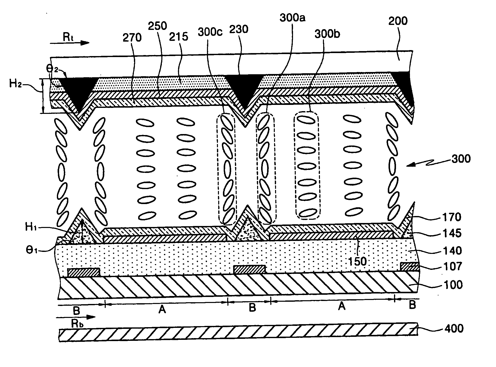
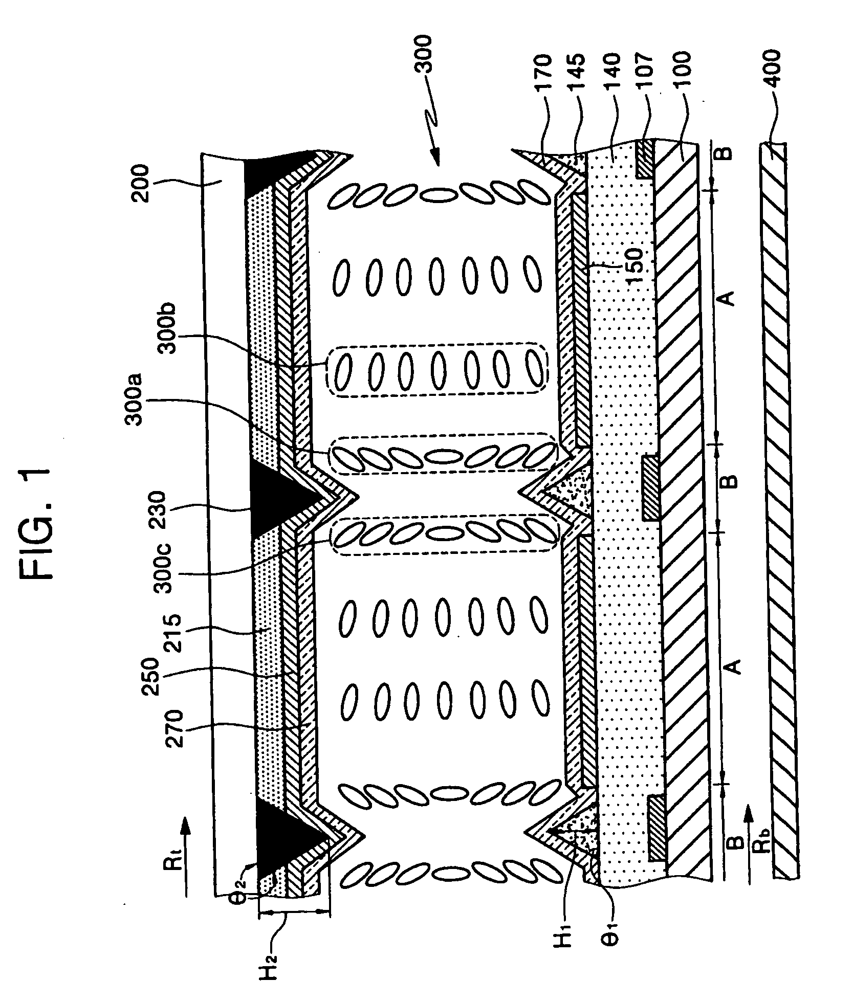
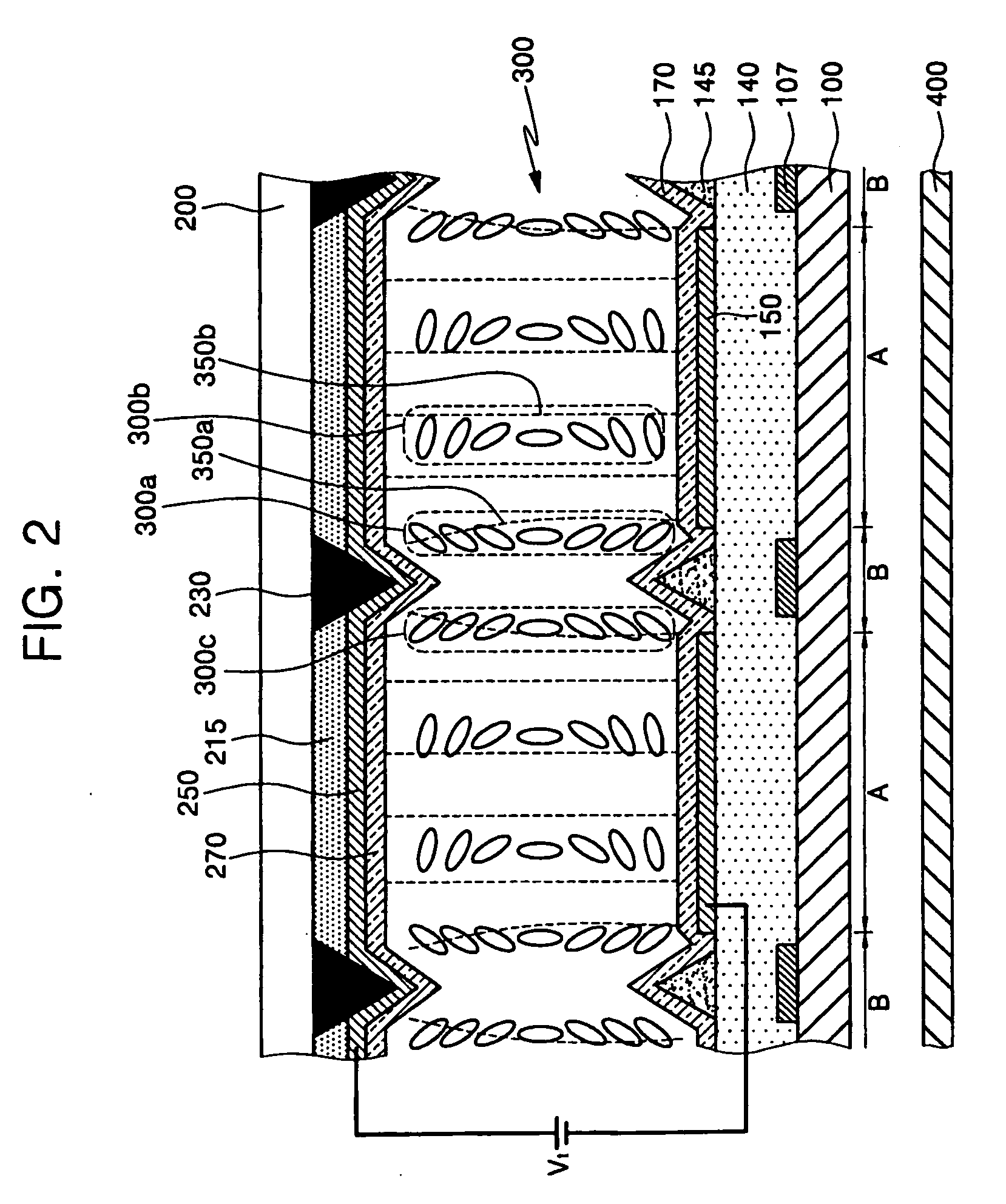
[0022] In the following detailed description, exemplary embodiments of the present invention are shown and described, by way of illustration. As those skilled in the art would recognize, the described exemplary embodiments may be modified in various ways, all without departing from the spirit or scope of the present invention. Accordingly, the drawings and description are to be regarded as illustrative in nature, rather than restrictive. There may be parts shown in the drawings, or parts not shown in the drawings, that are not discussed in the specification, as they are not essential to a complete understanding of the invention. Like reference numerals designate like elements. In a case where it is stated that one layer is formed “on” another layer, this may refer to the one layer being directly on the another layer or to a third layer being interposed between the one layer and the another layer.

[0023]FIG. 1 is a cross-sectional view illustrating an LCD device according to an embod...


PUM

PropertyMeasurementUnit
angleaaaaaaaaaa
angleaaaaaaaaaa
angleaaaaaaaaaa

Abstract

A liquid crystal display device and a method of fabricating the same are provided. The liquid crystal display device includes: a lower substrate having an opening region and a non-opening region adjacent to the opening region; a pixel electrode located on the opening region; an upper substrate located above the lower substrate and having an opposite surface facing the lower substrate; a protrusion type light shielding layer pattern located on a portion of the opposite surface corresponding to the non-opening region; an opposite electrode located on the protrusion type light shielding layer pattern; and an OCB mode liquid crystal layer located between the pixel electrode and the opposite electrode.

Description

CROSS-REFERENCE TO RELATED APPLICATION [0001] This application claims priority to and the benefit of Korean Patent Application No. 10-2004-0098250, filed on Nov. 26, 2004, the entire content of which is incorporated herein by reference. BACKGROUND OF THE INVENTION [0002] 1. Field of the Invention [0003] The present invention relates to a liquid crystal display (LCD) device and, more particularly, to an LCD device having an optically compensated bend (OCB) mode liquid crystal layer. [0004] 2. Description of the Related Art [0005] An LCD device has a liquid crystal injected between a pixel electrode and an opposite electrode, and changes alignment of the liquid crystal by forming an electric field between the pixel electrode and the opposite electrode. The changed alignment of the liquid crystal controls transmittance of light to form images. [0006] Of the various types of LCD devices, an optically compensated bend (OCB) type LCD device has a fast response speed and an excellent viewi...

Claims


Application Information

Patent Timeline
Patent Type & Authority Applications(United States)
IPC IPC(8): G02F1/1333
CPCG02F1/133512G02F1/133707G02F1/1395G02F1/1337
Inventor CHOI, KYUNG-HO
Owner SAMSUNG DISPLAY CO LTD
Why Eureka
Try Eureka