Semiconductor memory, memory controller and control method for semiconductor memory

a technology of semiconductor memory and memory controller, which is applied in the direction of information storage, static storage, digital storage, etc., can solve the problems of complex description content, difficult description per se, and difficult design, and achieve the effect of simplifying the related circuit configuration and easy design

Active Publication Date: 2009-10-06
SOCIONEXT INC
View PDF13 Cites 0 Cited by
  • Summary
  • Abstract
  • Description
  • Claims
  • Application Information

AI Technical Summary

Benefits of technology

[0012]The purpose of the present invention is to provide a memory control technique for enabling easy designs of semiconductor memory and a memory controller for controlling the memory for the semiconductor memory carrying out a synchronous transfer.
[0016]The first specific command is a Write command for example, and simplification of a command reception makes it possible to simplify a configuration of a circuit used for a control.
[0018]As such, the configuration for receiving a command only at every specific clock starting from the basis enables simplification of a circuit control.
[0020]This configuration makes it possible to separate between a control for defining an operation mode of the semiconductor memory and that for reading / writing data, thereby simplifying a control configuration.
[0022]This configuration is capable of preventing an erroneous change of an operation mode setup for the semiconductor memory.
[0024]The present invention enables easy designs of semiconductor memory and of a memory controller, and additionally simplification of the related circuit configurations. This in turn enables a design and a validation thereafter to be easy.

Problems solved by technology

A memory controller managing a control of memory is required to control SDRAM so as to satisfy various constraint conditions, making its design difficult.
Meanwhile, if a design is tried by describing such a specification by a hardware description language such as Verilog and VHDL (VHSIC (very high speed integrated circuit) description language), a description content becomes complex due to a cumbersomeness of the control.
Because of this, not only the description per se is difficult, but also an identification of the description with a specification is difficult to validate.

Method used


Image

  • Semiconductor memory, memory controller and control method for semiconductor memory
  • Semiconductor memory, memory controller and control method for semiconductor memory
  • Semiconductor memory, memory controller and control method for semiconductor memory

Examples


Embodiment Construction

[0035]The following is a description of the preferred embodiment of the present invention by referring to the accompanying drawings.

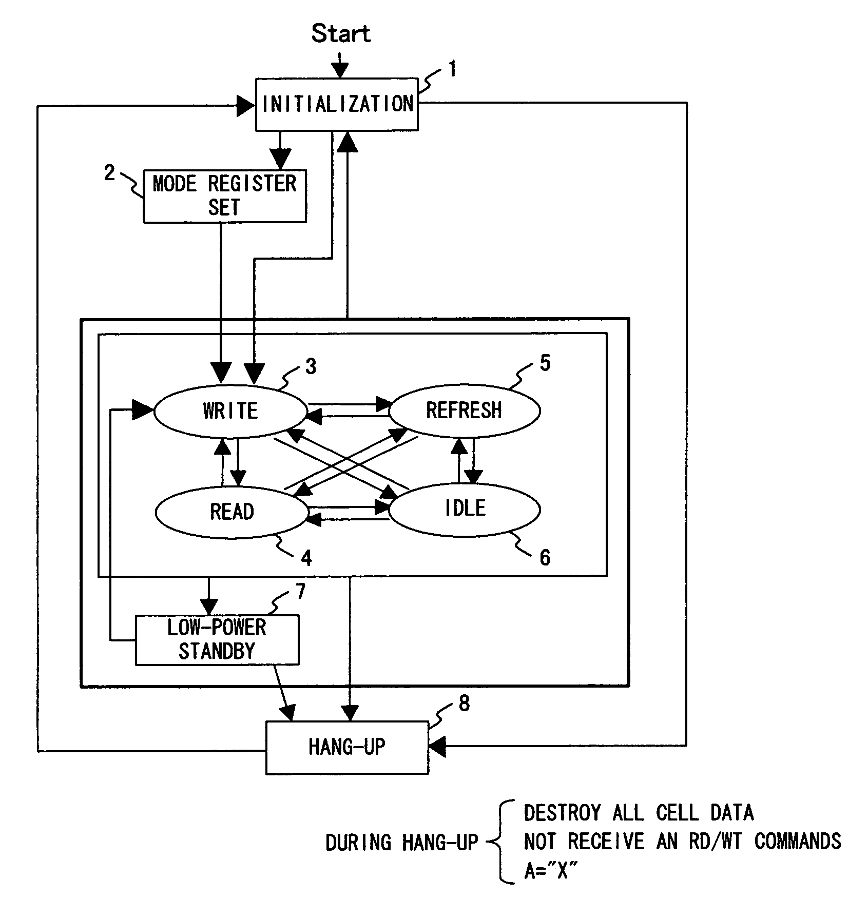
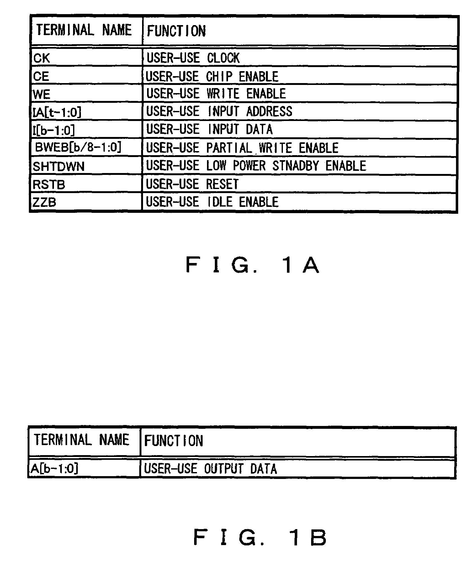
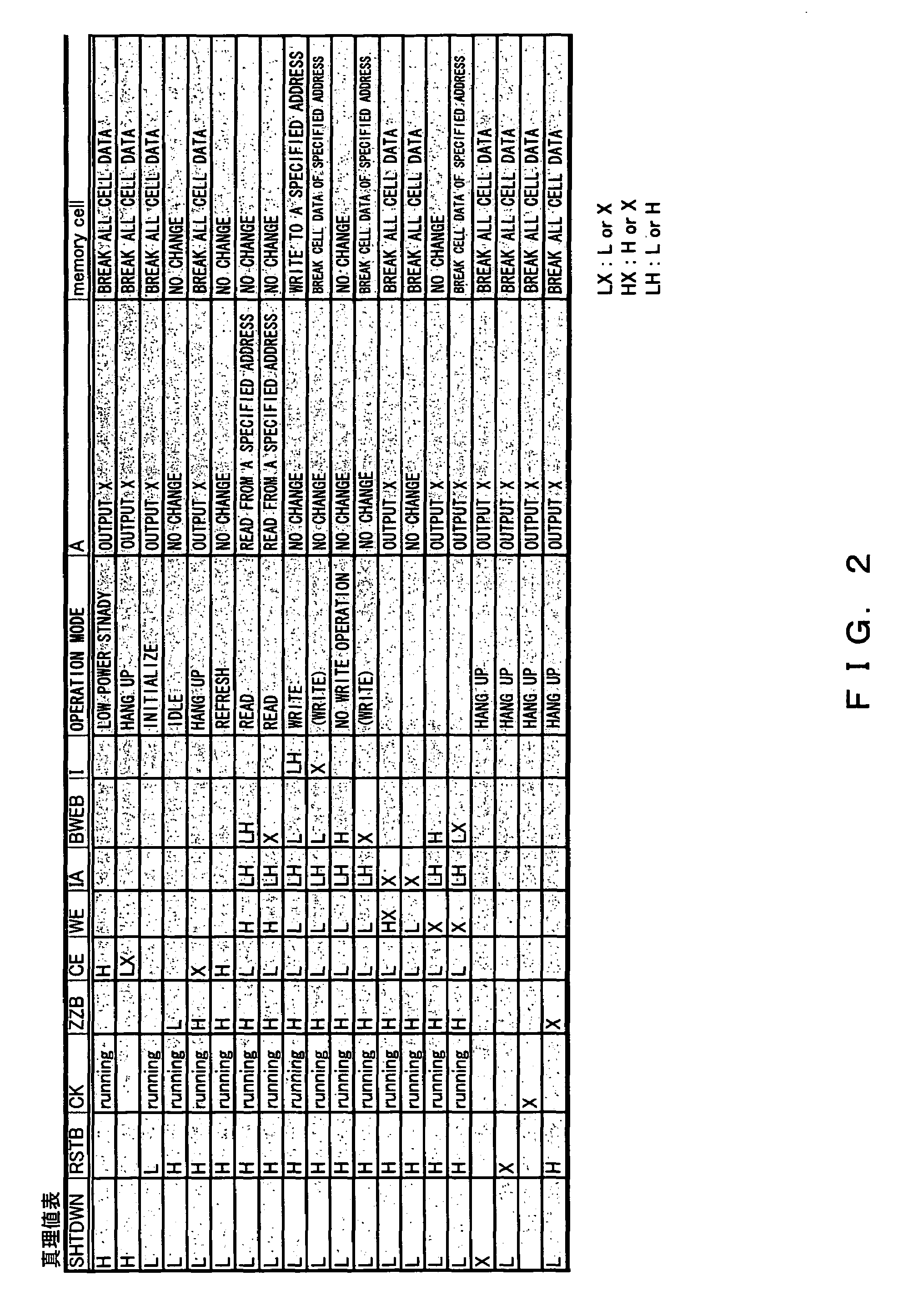
[0036]FIG. 1A is a chart exemplifying an input signal of memory according to the present embodiment; and FIG. 1B is a chart exemplifying an output signal of the memory according thereto. FIG. 2 is a chart exemplifying an active truth table corresponding to a state of an input signal.

[0037]According to the examples shown by FIGS. 1A and 1B, the memory used in the present embodiment comprises a clock CK, a chip enable CE, a Write enable WE, an input address IA [t−1: 0] (t denotes an address width), input data I [b−1: 0] (b denotes a data width), a partial Write enable BWEB [b / 8−1: 0], a low power standby enable SHTDWN, a reset RSTB and an idle enable ZZB as input signals; and comprises output data A [b−1: 0] as an output signal.

[0038]Among these, the clock CK is a clock signal used for synchronizing at the time of inputting and outputting data or command ...


PUM


Abstract

A semiconductor memory for inputting and outputting data synchronously with a clock includes a clock reception unit for receiving the clock, and a command reception unit for initially receiving a first specific command synchronizing with the clock after turning a power on, after a low-power standby or after an initialization, followed by starting a command reception.

Description

CROSS-REFERENCE TO RELATED APPLICATIONS[0001]This application is based upon and claims the benefit of priority from the prior Japanese Patent Application No. 2006-020427 filed on Jan. 30, 2006, the entire contents of which are incorporated herein by reference.BACKGROUND OF THE INVENTION[0002]1. Field of the Invention[0003]The present invention relates to a technique for controlling semiconductor memory of a synchronous transfer system.[0004]2. Description of the Related Art[0005]A burst transfer for raising a transfer speed by partially eliminating procedures such as specifying an address is one of effective means for improving a data transfer rate of semiconductor memory when transferring continuous data synchronously with a clock signal.[0006]For instance, a patent document 1 (Laid-Open Japanese Patent Application Publication No. 10-199233) has disclosed a method for implementing a burst transfer for EDO (extended data out) memory, which primarily performs an asynchronous transfer...

Claims


Application Information

Patent Timeline
Patent Type & Authority Patents(United States)
IPC IPC(8): G11C8/00
CPCG11C7/1072G11C7/225G11C7/22G11C7/20G11C11/4072G11C11/4076G11C11/4096
Inventor ETO, SATOSHIKAWABATA, KUNINORIMIYO, TOSHIYASERIZAWA, YUJI
Owner SOCIONEXT INC
Why Eureka
Try Eureka