
Making method for grid structure
A manufacturing method and gate structure technology, applied in the direction of semiconductor devices, etc., can solve the problems of increasing gates, device performance degradation, device failure, etc., to suppress the generation of gate root defects, uniform etching rate, and shorten the time interval Effect
Patent Information
- Authority / Receiving Office
- CN · China
- Patent Type
- Patents(China)
- Current Assignee / Owner
- Publication Date
- 2009-09-09
Smart Images
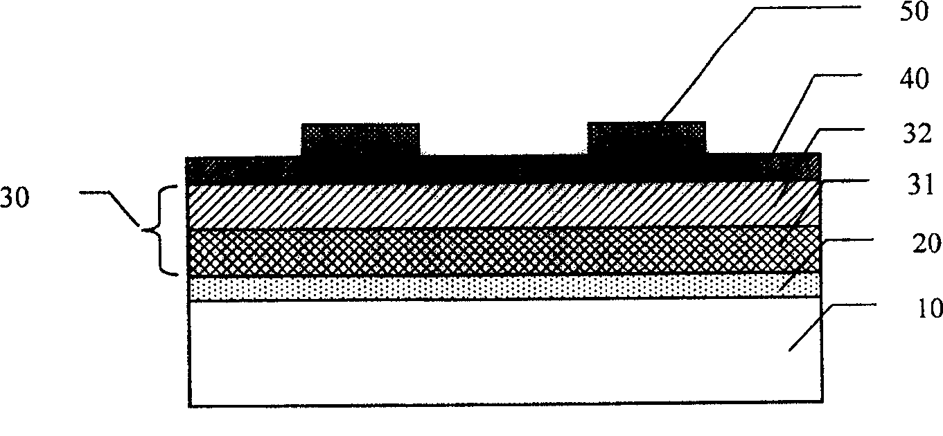
Figure 1 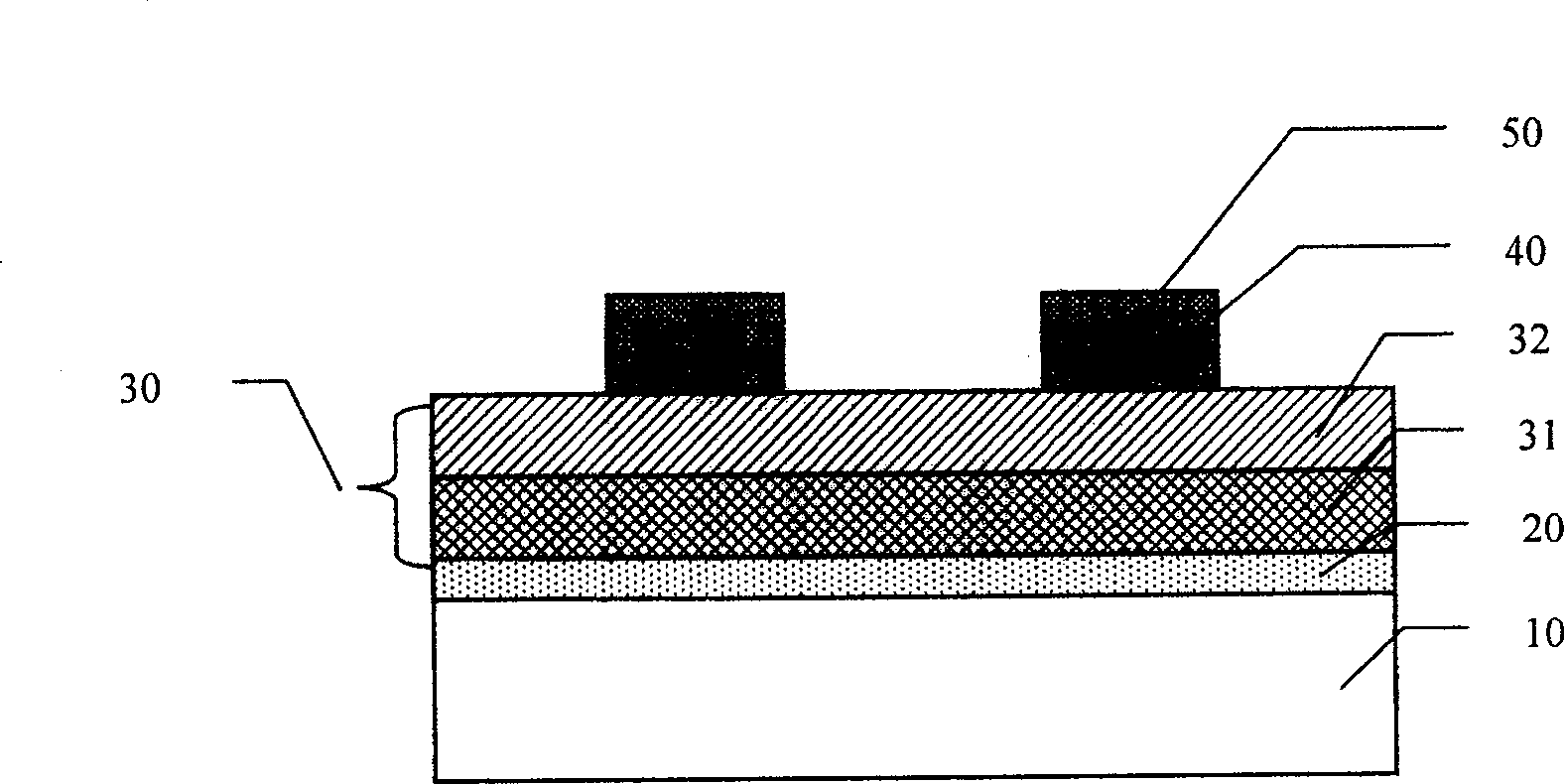
Figure 2 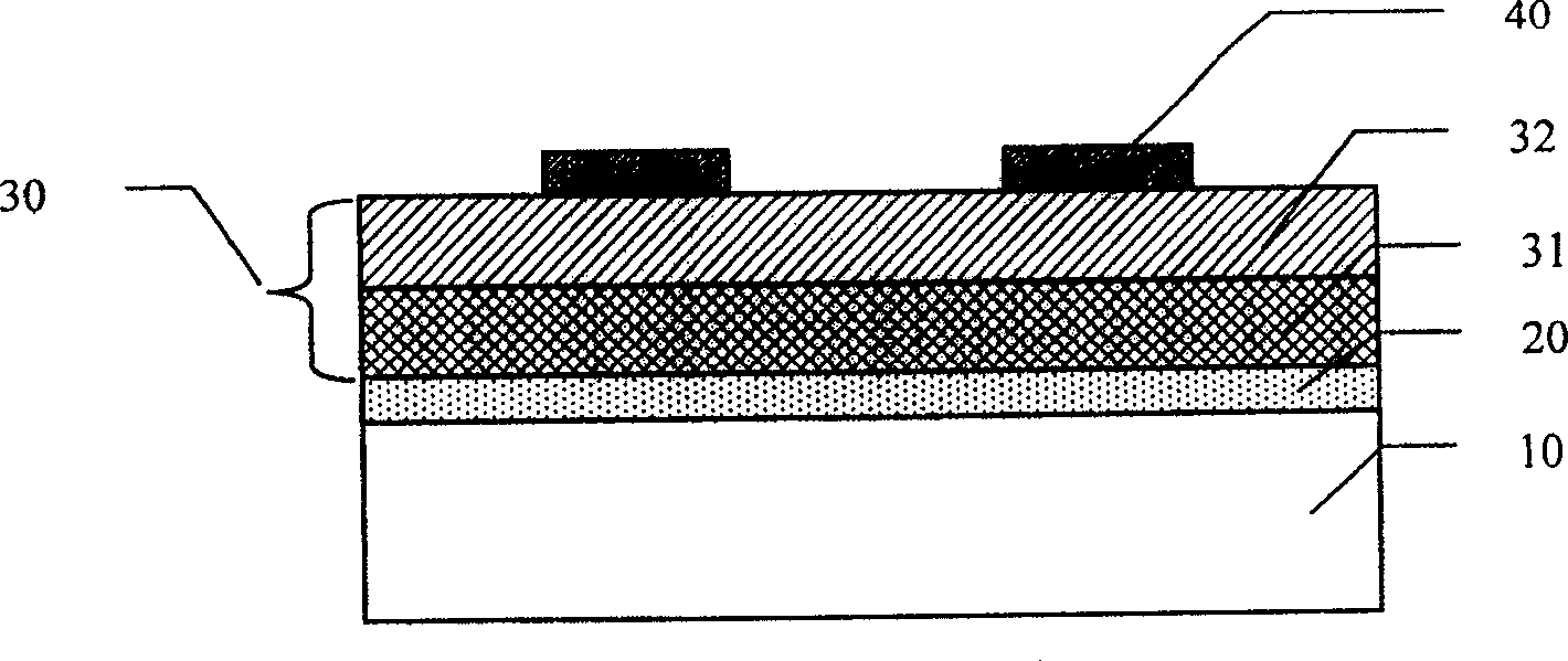
Figure 3
Abstract
Description
technical field
[0001] The invention relates to the technical field of semiconductor manufacturing, in particular to a method for manufacturing a gate structure. Background technique
[0002] Semiconductor devices change the electric field strength in the dielectric layer by applying a voltage on the gate, and then control the electric field on the surface of the substrate, and finally change the conductivity of the conductive channel. It can be seen that the performance of the gate is very important to the performance of the semiconductor device, and the performance of the gate is mainly determined by the structure of the gate.
[0003] Figure 1A-1D In order to illustrate the device cross-sectional diagram of each step of the manufacturing method of the gate structure in the prior art, as shown in the figure, a manufacturing method of the gate structure provided in the Chinese patent application with the application number "CN97111174.X" is as follows:
[0004] First, if ...
Examples
no. 3 example
[0061] As the third embodiment of the method of the present invention, its specific implementation steps include:
[0062] Firstly, a dielectric layer, a conductive layer, a barrier layer and a patterned photoresist layer are sequentially deposited on the substrate. Wherein, the conductive layer includes a polysilicon layer and a metal layer deposited sequentially.
[0063] Then, using the patterned photoresist layer as a mask, the blocking layer is etched to obtain a blocking layer with an opening area; the opening area of the blocking layer exposes the upper surface of the metal layer.
[0064] Afterwards, the patterned photoresist layer is removed to obtain a smooth upper surface of the barrier layer and the metal layer.
[0065] Subsequently, the metal oxide is etched using the barrier layer with the opening region as a mask.
[0066] As an embodiment of the method of the present invention, the time interval between the removal of the patterned photoresist layer and th...