
Wafer wet etching equipment
A wet etching, wafer technology, used in electrical components, semiconductor/solid-state device manufacturing, circuits, etc., can solve problems such as large differences in etching rates in different chambers
Patent Information
- Authority / Receiving Office
- CN · China
- Patent Type
- Applications(China)
- Current Assignee / Owner
- Publication Date
- 2021-09-14
Smart Images
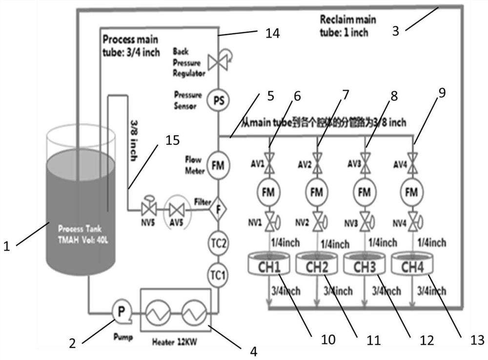
Figure 1 
Figure 2 
Figure 3
Abstract
Description
technical field
[0001] The invention relates to the field of semiconductor integrated circuit manufacturing, in particular to a wafer wet etching equipment. Background technique
[0002] In the manufacture of semiconductor devices, etching processes include dry etching and wet etching. In dry etching, the etching gas is usually fed into the etching chamber, and plasma is formed to form plasma (plasma), and then the etched material on the wafer, such as a silicon wafer, is etched. Wet etching uses an etching solution to etch the material to be etched on the wafer.
[0003] With the continuous development of semiconductor technology, the process node, that is, the line width will continue to shrink, and the technology of line width restriction will make the process more and more difficult. In order to reduce the damage of the metal gate layer or the surface of the film (film), the existing dry etching The requirements for etching technology are becoming increasingly stringen...
Examples
Embodiment Construction
[0028] The wafer wet etching equipment structure of specific embodiment of the present invention sees figure 1 .
[0029] figure 1 Among them, NV is the needle valve (Needle Valve); AV is the air valve (Air Valve); TC is the temperature controller (Temperature Controller); FM is the flow meter (Flow meter).
[0030] The wafer wet etching equipment includes an etchant, which is placed in a storage container 1, and the usual storage capacity is 40L. In this embodiment, the etchant is TMAH tetramethylammonium hydroxide.
[0031] The pipelines connected with the storage container 1 include a main pipeline 5 , a pressure relief pipeline 14 , an auxiliary pipeline 15 and a recovery pipeline 3 . The main pipeline 5 includes a pump 2, a heater 4, a flow meter, a temperature controller and the like. The pressure relief pipeline 14 includes a pressure sensor, a pressure regulator and the like.
[0032] The heater 4 is used to control the temperature of the etchant on the main pipeli...