
Organic resistive random access memory and preparation method thereof
A resistive memory, organic technology, applied in the field of memory, can solve problems such as poor chemical stability and thermal stability, and achieve the effects of excellent mechanical properties, good thermal stability, and stable resistive characteristics
Patent Information
- Authority / Receiving Office
- CN · China
- Patent Type
- Applications(China)
- Current Assignee / Owner
- Publication Date
- 2013-07-24
- Estimated Expiration
- Not applicable · inactive patent
Smart Images
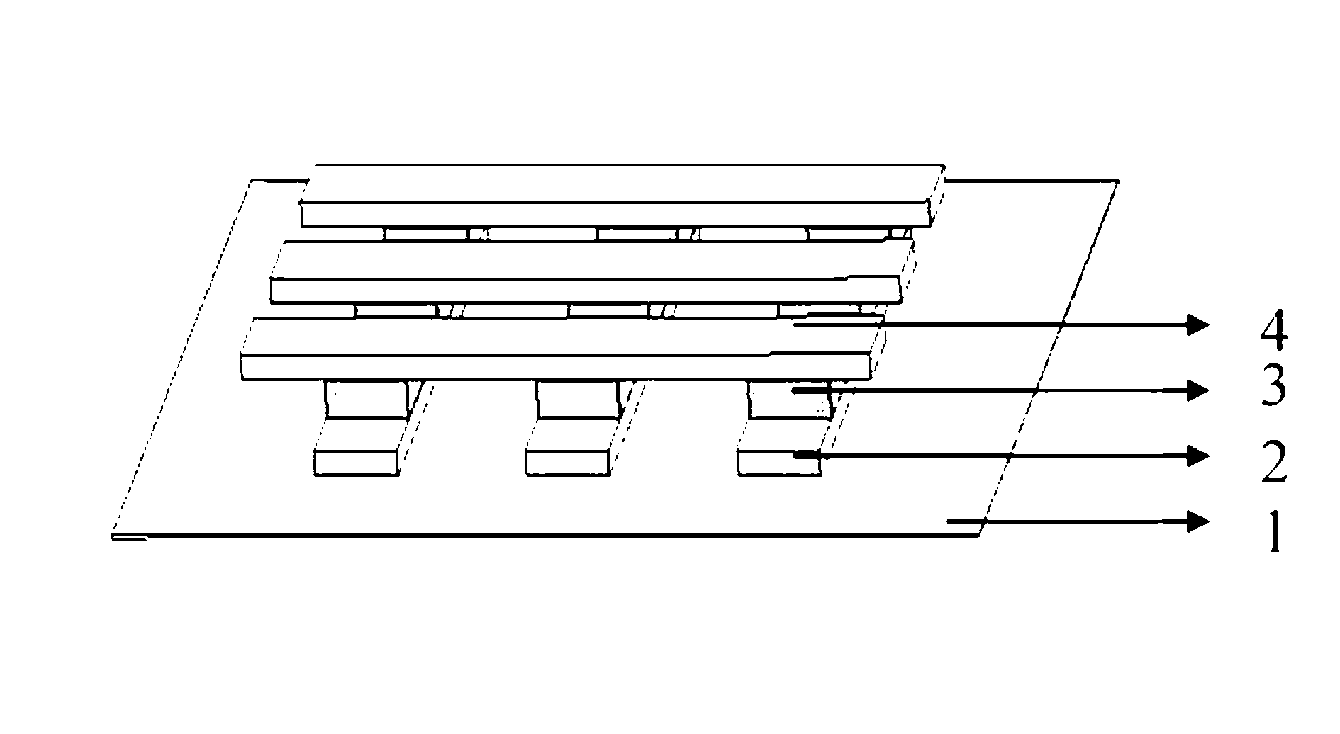
Figure 1 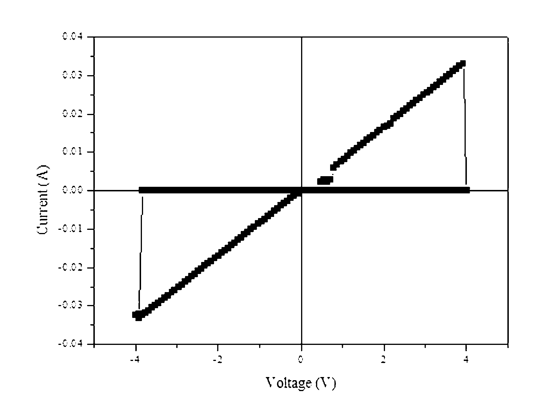
Figure 2 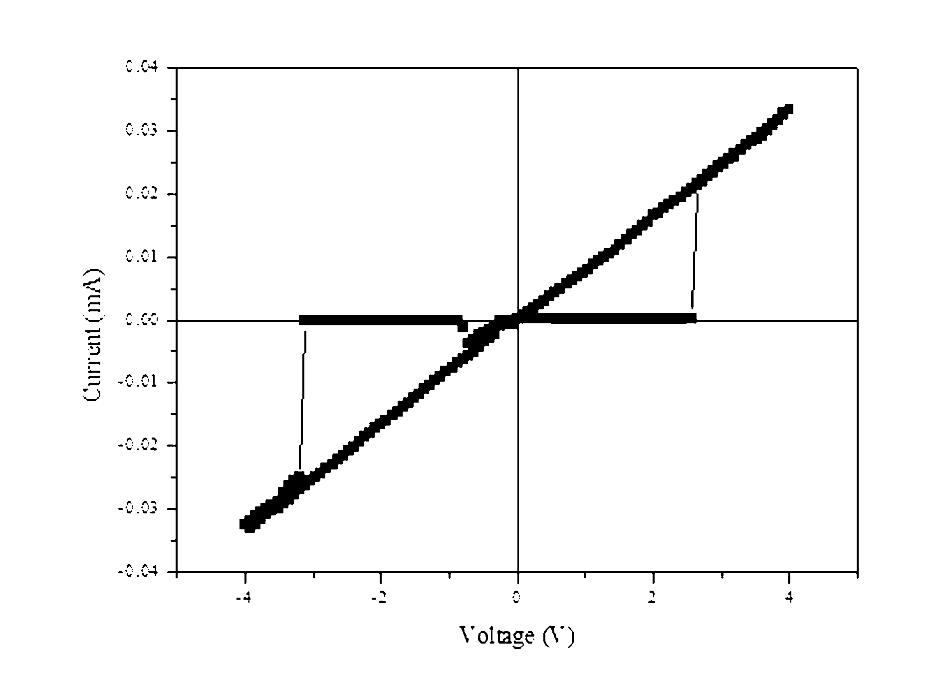
Figure 3
Abstract
Description
technical field
[0001] The invention belongs to the technical field of memory, and in particular relates to an organic resistive variable memory and a preparation method thereof. Background technique
[0002] With the vigorous development of information technology, all kinds of consumer electronic products are developing rapidly. The volume of electronic products is developing towards miniaturization, while the demand for storage capacity is developing towards the direction of large capacity. At present, Flash memory is the main memory, but the development of Flash memory based on the charge storage mechanism is limited as the size of the device continues to shrink. As the thickness of the tunneling layer decreases, the charge leakage will become more and more serious, which will directly affect the performance of the Flash memory. With the development of the traditional memory cell structure approaching the limit of physical size, a variety of new non-volatile memories ha...
Examples
Embodiment 1
[0032] use figure 1 The array memory structure shown is used to prepare an organic resistive variable memory, which includes a substrate material 1 , a lower electrode 2 , an organic resistive variable layer 3 and an upper electrode 4 from bottom to top.
[0033] Its preparation method is:
[0034] (1) Use glass as the substrate, ultrasonically clean it with deionized water, acetone and alcohol, and dry it with hot air for later use;
[0035] (2) The substrate is prepared with a strip-shaped metal Al lower electrode by evaporation process, with a line width of 80 μm and a thickness of 150 nm;
[0036] (3) Preparation of organic resistive layer:
[0037] Dissolve PEI in chloroform, then drop the PEI solution into MMA, and stir evenly, add 1wt% initiator BPO (benzoyl peroxide) or AIBN (azobisisobutyronitrile), heat up to 75 Stir at ~85°C for 3 hours, then raise the temperature to 125°C and stir for 30 minutes to obtain a blend solution of PMMA prepolymer and PEI, add chloro...
Embodiment 2
[0042] use figure 1 In the array storage structure shown, the strip-shaped metal Ag lower electrode is prepared by evaporation process on the glass substrate, with a line width of 80 μm and a thickness of 80 nm. Dissolve PEI in chloroform, then drop PEI solution into MMA, and stir evenly, add 1wt% initiator BPO (benzoyl peroxide) or AIBN (azobisisobutyronitrile), heat up to 75 Stir at ~85°C for 3 hours, then raise the temperature to 125°C and stir for 30 minutes to obtain a blend solution of PMMA prepolymer and PEI, add chloroform for dilution, and synthesize a molecular level blend. The above solution was spin-coated and deposited on the bottom electrode prepared with the bottom electrode, and then placed in a vacuum oven at 120° C. for curing reaction for 20 minutes to form an organic resistive film with a thickness of about 140 nm. Finally, strip-shaped metal Ag was evaporated on the surface of the organic film superior The electrode has a line width of 80 μm and a thi...
Embodiment 3
[0045] Use PET as the substrate, ultrasonically clean with deionized water, dry with hot air, and then treat the surface with ultraviolet ozone. The substrate is prepared with a strip-shaped metal Ag lower electrode by an evaporation process, with a line width of 80 μm and a thickness of 80 nm. Dissolve PEI in chloroform, then drop the PEI solution into MMA, and stir evenly, add 1wt% initiator BPO (benzoyl peroxide) or AIBN (azobisisobutyronitrile), heat up to 75 Stir at ~85°C for 3 hours, then raise the temperature to 125°C and stir for 30 minutes to obtain a blend solution of PMMA prepolymer and PEI, add chloroform for dilution, and synthesize a molecular level blend. The above solution was spin-coated and deposited on the bottom electrode prepared with the bottom electrode, and then placed in a vacuum oven at 120° C. for curing reaction for 20 minutes to form an organic resistive film with a thickness of about 140 nm. Finally, strip-shaped metal Al is evaporated on the sur...