
Method for preparing suede-like surface structure of crystalline silicon solar cell
A technology of solar cells and crystalline silicon, applied in the field of solar cells, can solve the problems of unsuitable industrial production and low conversion efficiency of cells, and achieve the effects of reducing processing costs, being suitable for popularization and application, and having obvious advantages in efficiency
Patent Information
- Authority / Receiving Office
- CN · China
- Patent Type
- Applications(China)
- Current Assignee / Owner
- Publication Date
- 2015-10-14
- Estimated Expiration
- Not applicable · inactive patent
Smart Images
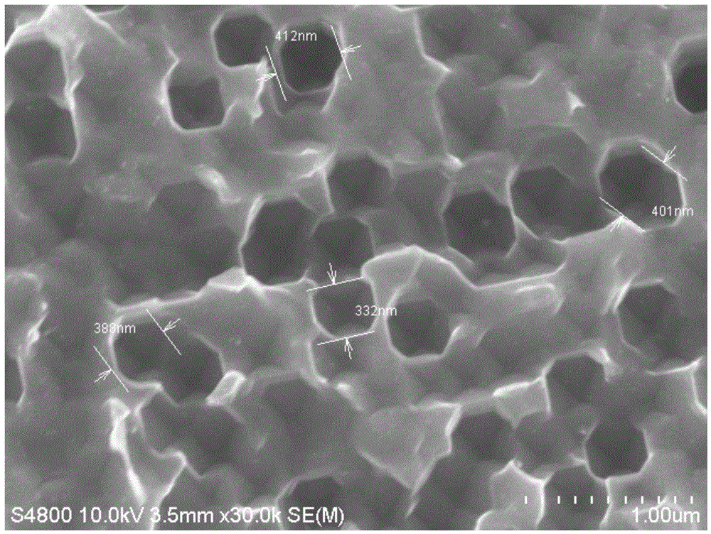
Figure 1 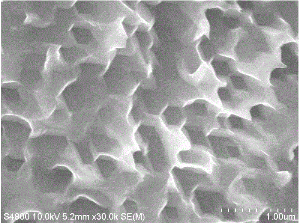
Figure 2 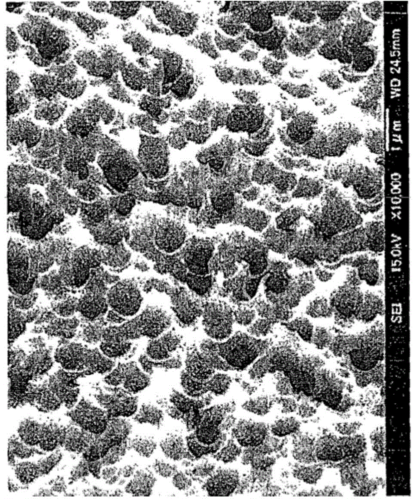
Figure 3
Abstract
Description
technical field
[0001] The invention relates to a method for preparing a textured surface structure of a crystalline silicon solar cell, belonging to the technical field of solar cells. Background technique
[0002] With the wide application of solar cell components, photovoltaic power generation occupies an increasingly important proportion in new energy and has achieved rapid development. Among the current commercialized solar cell products, crystalline silicon (monocrystalline and polycrystalline) solar cells have the largest market share, maintaining a market share of more than 85%.
[0003] At present, in the production process of solar cells, the textured structure on the surface of silicon wafers can effectively reduce the surface reflectance of solar cells, which is one of the important factors affecting the photoelectric conversion efficiency of solar cells. In order to obtain a good textured structure on the surface of crystalline silicon solar cells to achieve a ...
Examples
Embodiment 1
[0037] A method for preparing a textured structure of a polycrystalline silicon solar cell, comprising the following steps:
[0038] (1) Clean the silicon wafer and remove the surface damage layer;
[0039] (2) Put the above-mentioned silicon chip into a chemical etching solution containing metal ions to form nanowires or porous silicon structures on the surface of the silicon chip; the temperature is 30°C, and the time is 200 seconds;
[0040] The metal ion is selected from silver ion;
[0041] The chemical etching solution is selected from HF and H 2 CrO 4 mixed solution; wherein, the concentration of HF is 10 mol / L, H 2 CrO 4 The concentration is 0.4 mol / L;
[0042] (3) Putting the above-mentioned silicon chip into the first chemical etching solution for corrective etching, so that the above-mentioned nanowire or porous silicon structure forms a nano-deep hole structure;
[0043] The first chemical etching solution is H 2 CrO 4 and HF mixed acid solution, wherein th...
Embodiment 2
[0055]A method for preparing a textured structure of a polycrystalline silicon solar cell, comprising the following steps:
[0056] (1) Clean the silicon wafer and remove the surface damage layer;
[0057] (2) Put the above-mentioned silicon chip into a chemical etching solution containing metal ions to form nanowires or porous silicon structures on the surface of the silicon chip; the temperature is 30°C, and the time is 200 seconds;
[0058] The metal ion is selected from silver ion;
[0059] The chemical etching solution is selected from HF and H 2 CrO 4 mixed solution; wherein, the concentration of HF is 10 mol / L, H 2 CrO 4 The concentration is 0.4 mol / L;
[0060] (3) Putting the above-mentioned silicon chip into a chemical etching solution for corrective etching, so that the above-mentioned nanowire or porous silicon structure forms a nano-concave structure;
[0061] The chemical corrosion solution is selected from tetramethylammonium hydroxide solution; its concent...