
Multi-quantum well layer growing method of micro LED
A multi-quantum well layer and growth method technology, which is applied in the field of microLED multi-quantum well layer growth, can solve the problems of poor crystallization quality and poor electrical parameters of the quantum well layer structure, so as to improve antistatic ability and leakage performance, improve Effects of crystal quality and dislocation density reduction
Patent Information
- Authority / Receiving Office
- CN · China
- Current Assignee / Owner
- Publication Date
- 2018-03-23
- Estimated Expiration
- Not applicable · inactive patent
Smart Images
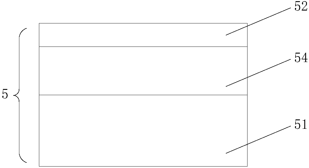
Figure 1 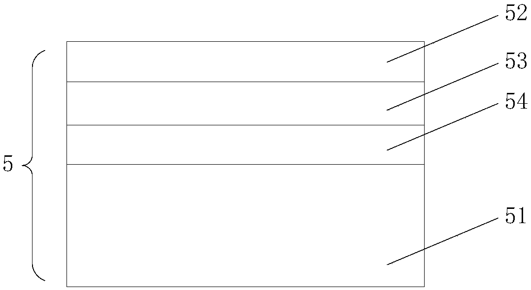
Figure 2 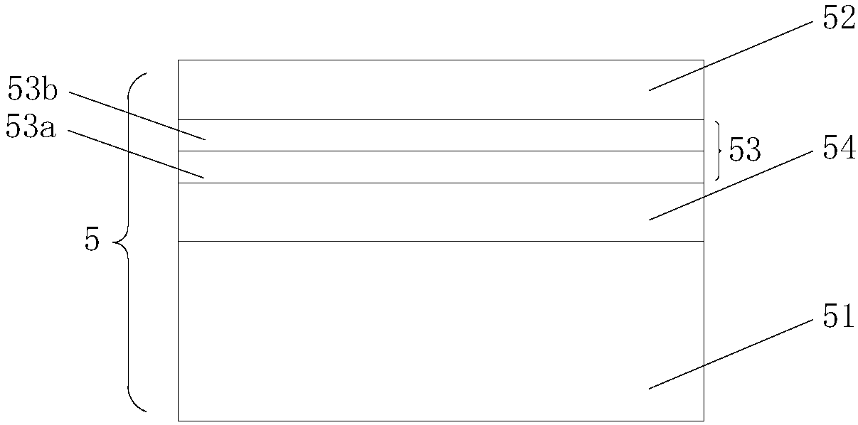
Figure 3
Abstract
Description
technical field
[0001] The invention relates to the technical field of microLEDs, in particular to a method for growing a microLED multi-quantum well layer. Background technique
[0002] The display principle of MicroLED Display is to make the LED structure design into thin film, miniaturization, and array. On the transparent and opaque substrates; and then use the physical deposition process to complete the protective layer and the upper electrode, and then the upper substrate can be packaged to complete a Micro LED display with a simple structure.
[0003] To make a display, the surface of the wafer must be made into an array structure like an LED display, and each pixel must be addressable and controllable, and driven to light up individually. If it is driven by a complementary metal oxide semiconductor circuit, it is an active addressing drive architecture. The MicroLED array chip and the CMOS can be packaged through packaging technology. After the paste is completed, t...
Examples
Embodiment Construction
[0021] In order to make the object, technical solution and advantages of the present invention clearer, the implementation manner of the present invention will be further described in detail below in conjunction with the accompanying drawings.
[0022] The present invention provides a microLED multi-quantum well layer growth method, see figure 1 , the multi-quantum well layer 5 includes GaN barrier layer 51 and In x Ga 1-x N well layer 52, 0x Ga 1-x No hydrogen gas is injected into the N well layer 52 during the process.
[0023] Introducing hydrogen gas during the formation of the microLED epitaxial structure can effectively improve the crystal quality of GaN, but when growing multiple quantum well layers, due to the In x Ga 1-x The N well layer 52 contains In components, and the introduction of hydrogen will destroy the In structure, thereby reducing the luminous efficiency. In the prior art, when growing the GaN barrier layer 51, the In x Ga 1-x In the same atmosphere...