
Microlens array imaging system
A technology of microlens array and imaging system, which is applied in the field of imaging system, can solve the problems of information loss, long image processing time, large manpower and time consumption, etc., achieve small amount of calculation for data processing, improve the overall resolution, and avoid mutual interference Effect
Patent Information
- Authority / Receiving Office
- CN · China
- Patent Type
- Applications(China)
- Current Assignee / Owner
- Publication Date
- 2018-10-09
- Estimated Expiration
- Not applicable · inactive patent
Smart Images
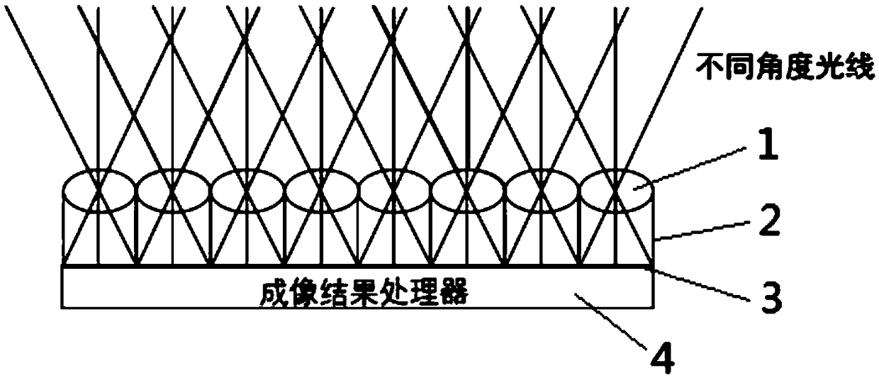
Figure 1 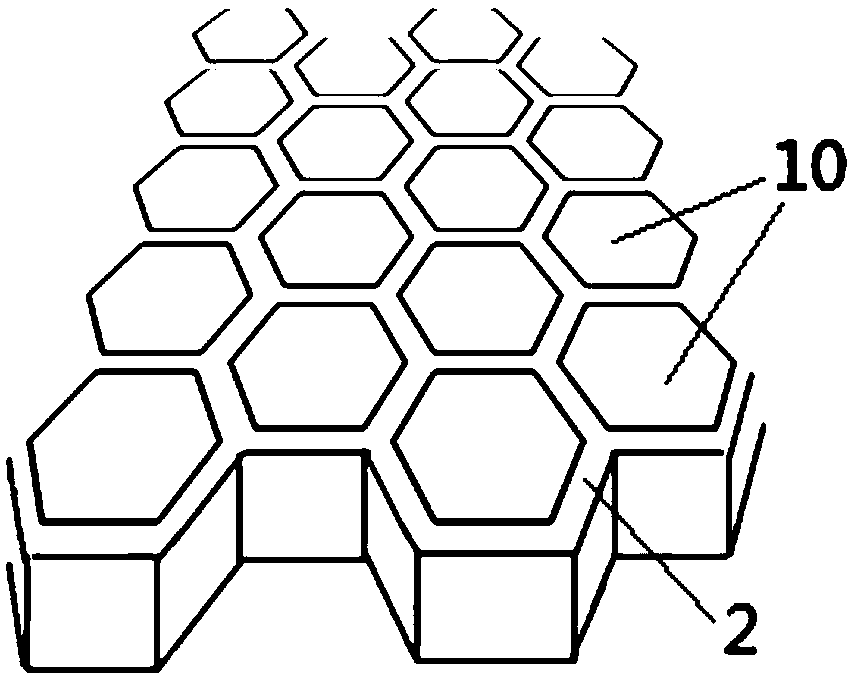
Figure 2 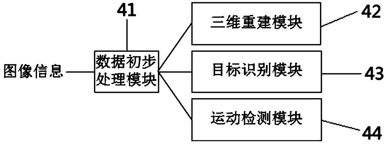
Figure 3
Abstract
Description
technical field
[0001] The invention relates to an imaging system, in particular to a microlens array imaging system. Background technique
[0002] Most of the cameras currently on the market have a single main lens, which converts the three-dimensional real world into a two-dimensional image, resulting in a large amount of information loss. However, in order to restore three-dimensional information from two-dimensional image information, it is mostly difficult to perform three-dimensional reconstruction. Therefore, a camera capable of collecting light fields is urgently needed to solve this problem.
[0003] At present, the cameras with the function of collecting light field are mainly camera arrays and light field cameras on the market. Among them, the problem of the camera array is that it is large in size, and it takes a lot of manpower and time to adjust the relative positions of the cameras; while the light field camera is It is an integrated structure, which uses a m...
Examples
Embodiment Construction
[0019] Below in conjunction with the drawings, preferred embodiments of the present invention are given and described in detail.
[0020] Such as Figure 1-3 As shown, the present invention, that is, a microlens array imaging system, includes: a microlens array 1, an opaque light-shielding processing structure 2, a photosensitive pixel array 3, and an imaging result processor 4, specifically:
[0021] The microlens array 1 includes a plurality of microlenses 10 arranged adjacent to each other, and each microlens 10 is hexagonal;
[0022] The light-shielding processing structure 2 is arranged between every two adjacent microlenses 10, that is, the periphery of each microlens 10 has a light-shielding processing structure 2, thereby forming a planar or curved honeycomb shape together with a plurality of microlenses 10. grid structure;
[0023] The photosensitive pixel array 3 is used to receive the light transmitted by the microlens array 1, and form an electrical signal that i...