
A compact multi-band antenna
A multi-band antenna, compact technology, applied in the direction of antenna, antenna grounding device, antenna grounding switch structure connection, etc., can solve the problems of difficult integration, narrow frequency band bandwidth, affecting antenna performance, etc., to meet broadband and multi-band, easy Integrated, small size effect
Patent Information
- Authority / Receiving Office
- CN · China
- Patent Type
- Patents(China)
- Current Assignee / Owner
- Publication Date
- 2021-07-16
Smart Images
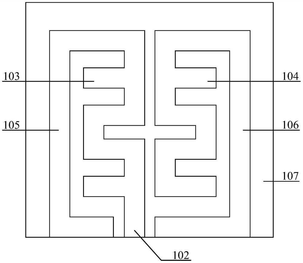
Figure 1 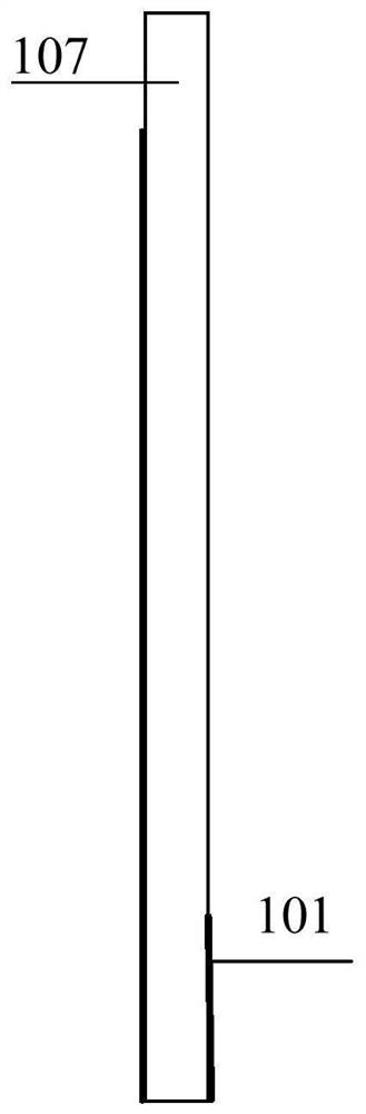
Figure 2 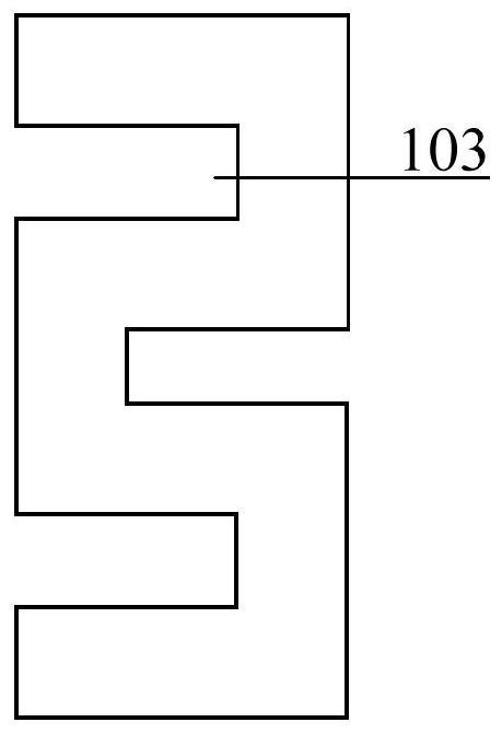
Figure 3
Abstract
Description
technical field
[0001] The invention belongs to the field of wireless mobile communication, and in particular relates to a compact multi-band antenna. Background technique
[0002] With the gradual improvement of people's living standards, the dependence on electronic products is becoming stronger and stronger, and mobile communication devices such as mobile phones, computers, and tablet computers are more and more widely used in people's daily life. And with the advancement of technology and the more stable and mature manufacturing process, the miniaturization of mobile communication equipment has become a development trend, and higher requirements have been proposed for antennas that connect the internal components of mobile communication equipment with the external environment. Requirements, the development of miniaturization, integration, broadband, multi-band and other directions will be the trend of antenna design in the future. In wireless mobile communication system...
Examples
Embodiment Construction
[0028] The present invention will be further described below in conjunction with the accompanying drawings.
[0029] The present invention provides a compact multi-band antenna, including a dielectric substrate 107, a microstrip transmission line 102 disposed on the dielectric substrate 107, a first bow-shaped radiation unit 103, a second anti-bow-shaped radiation unit 104, and a third C-shaped radiation unit 105 and the fourth anti-C-shaped radiation unit 106 , and part of the ground plane 101 disposed on the back of the dielectric substrate 107 . The first bow-shaped radiation unit 103 and the second anti-bow-shaped radiation unit 104 are formed by bending a rectangular microstrip line multiple times, the first bow-shaped radiation unit 103 is directly connected to the microstrip transmission line 102 for feeding, and the third C-shaped radiation unit 105 is connected to the The first bow-shaped radiation unit 103 is directly connected to feed power. The second anti-bow rad...