

Manufacturing method of semiconductor device
A manufacturing method and semiconductor technology, applied in the direction of semiconductor/solid-state device manufacturing, semiconductor devices, electrical components, etc., can solve the problems of increased junction leakage current and performance degradation of semiconductor devices, so as to reduce junction capacitance and junction leakage current and improve good performance. rate and performance, avoiding the effects of lateral diffusion
Patent Information
- Authority / Receiving Office
- CN · China
- Patent Type
- Applications(China)
- Current Assignee / Owner
- Publication Date
- 2018-12-25
Smart Images
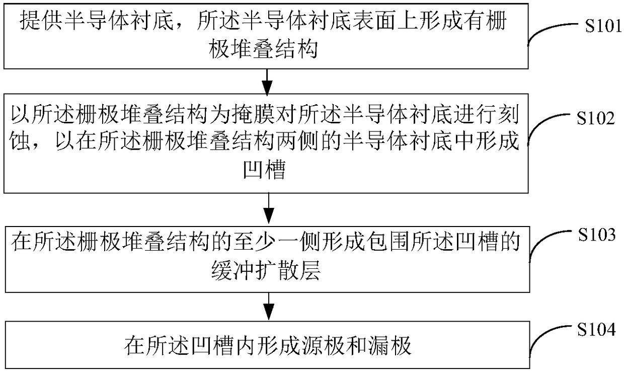
Figure 1 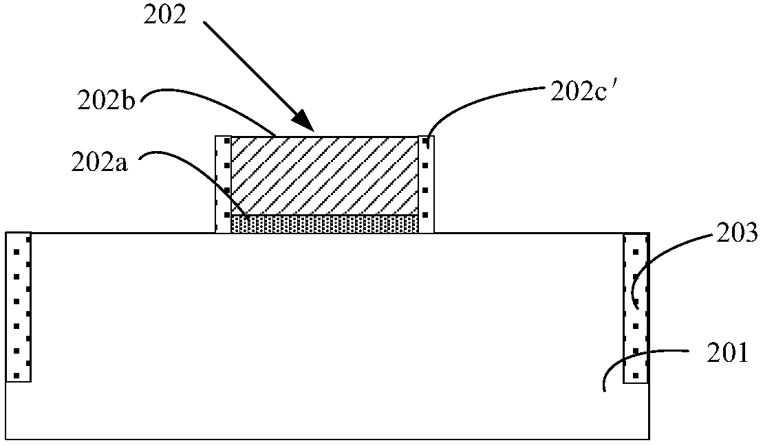
Figure 2 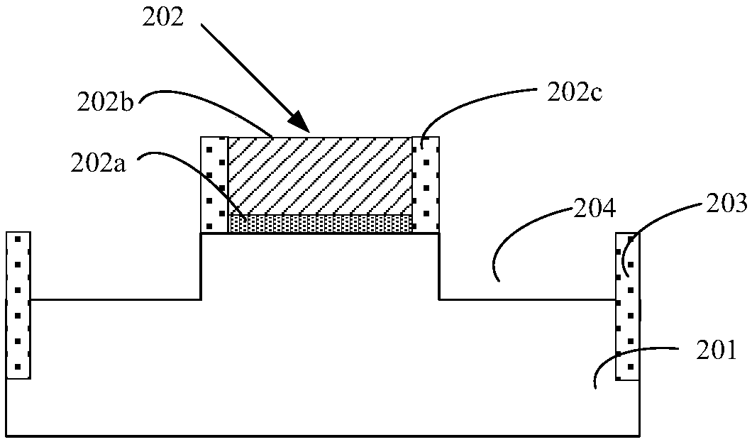
Figure 3
Abstract
Description
technical field
[0001] The invention relates to the technical field of semiconductors, in particular to a method for manufacturing a semiconductor device. Background technique
[0002] As the feature size of metal-oxide-semiconductor (metal oxide semiconductor, MOS) field effect transistor devices continues to decrease, it becomes more and more important to effectively control the channel length of MOS devices during their fabrication. challenge. For this reason, the short-channel effect of core devices can be improved by adopting the method of forming ultra-shallow junctions and abrupt junctions in MOS devices. However, in the process of forming ultra-shallow junctions and abrupt junctions, how to find a more reasonable balance between suppressing the Short Channel Effect (SCE) and improving the performance of MOS devices is also an extremely challenging task.
[0003] In order to further improve the performance of MOS devices, those skilled in the art are devoting themse...
Examples
Embodiment 1
[0039] Take P-type Metal-Oxide-Semiconductor Field-Effect Transistor (Metal-Oxide-Semiconductor Field-Effect Transistor, MOSFET) as an example, refer to Figure 2A-Figure 2E , which shows schematic cross-sectional views of semiconductor devices respectively obtained by sequentially implementing steps according to the method of Embodiment 1 of the present invention.
[0040] First, if Figure 2A As shown, a semiconductor substrate 201 is provided, and a gate stack structure 202 is formed on the surface of the semiconductor substrate 201, and then a lightly doped process (Lightly Doped Drain, LDD) is used to inject The region of the gate stack structure 202 is ion implanted and annealed to form a lightly doped drain (LDD) ion implantation region (not shown in the figure) in the region of the semiconductor substrate 201 adjacent to the gate stack structure 202 .
[0041]Further, the constituent material of the semiconductor substrate 201 can be undoped single crystal silicon, si...
Embodiment 2
[0061] Taking P-type metal-oxide semiconductor field-effect transistor (Metal-Oxide-Semiconductor Field-Effect Transistor, MOSFET) as an example, refer to Figure 3A-Figure 3F , which shows schematic cross-sectional views of semiconductor devices respectively obtained by sequentially implementing steps according to the method of Embodiment 2 of the present invention.
[0062] First, if Figure 3A As shown, a semiconductor substrate 301 is provided, and a gate stack structure 302 is formed on the surface of the semiconductor substrate 301, and then a lightly doped process (Lightly Doped Drain, LDD) is used to lightly doped the semiconductor substrate 301 adjacent to the gate The region of the gate stack structure 302 is ion implanted and annealed to form a lightly doped drain (LDD) ion implantation region (not shown in the figure) in the region of the semiconductor substrate 301 adjacent to the gate stack structure 302 .
[0063] Further, the constituent material of the semico...