
Fin-type super junction power semiconductor transistor and preparation method thereof
A technology for power semiconductors and transistors, which is applied in the field of fin-type super-junction power semiconductor transistors and their preparation, and can solve problems such as failure to achieve
Patent Information
- Authority / Receiving Office
- CN · China
- Patent Type
- Patents(China)
- Current Assignee / Owner
- Publication Date
- 2021-07-09
Smart Images
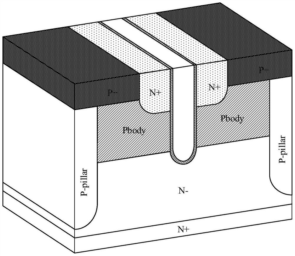
Figure 1 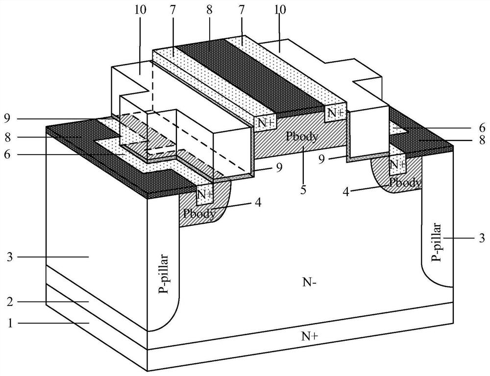
Figure 2 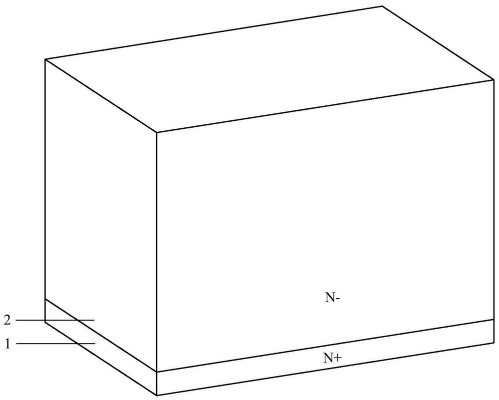
Figure 3
Abstract
Description
technical field
[0001] The invention relates to the technical field of power semiconductor devices, in particular to a fin-type super junction power semiconductor transistor and a preparation method thereof. Background technique
[0002] Power semiconductor devices, as the core components in power electronic systems, have been indispensable and important electronic components in modern life since their invention in the 1970s. In the past three decades, power metal oxide semiconductor field effect transistors (MOSFETs) have achieved leapfrog development. In the early 1990s, the concept of "super junction" was proposed, using alternate P columns and N columns to replace the traditional The N drift region of the power device effectively reduces the on-resistance and obtains lower on-state power consumption. Compared with traditional MOSFETs, although field effect transistors with super-junction structures have performed well in reducing on-resistance, they still have not met i...
Examples
Embodiment 1
[0027] Combine below figure 2 , the present invention is described in detail, a fin-type super junction power semiconductor transistor, comprising: an N-type substrate 1, an N-type epitaxial layer 2 is arranged on the N-type substrate 1, and both sides of the N-type epitaxial layer 2 Columnar first P-type body regions 3 are respectively provided, and second P-type body regions 4 are respectively provided on both sides of the N-type epitaxial layer 2. The columnar first P-type body regions 3 and the second P-type body regions on the same side Type body region 4 touches each other, a first N-type heavily doped source region 6 is provided on the surface of the second P-type body region 4, a third P-type body region 5 is provided on the top of the N-type epitaxial layer 2, and a third P-type body region 5 is provided on the surface of the second P-type body region 4. Both ends of the surface of the P-type body region 5 are respectively provided with second N-type heavily doped so...
Embodiment 2
[0029] Combine below Figure 3 ~ Figure 8 , the present invention is described in detail, a method for preparing a fin-type super-junction power semiconductor transistor:
[0030] The first step: first select N-type silicon material as the substrate and epitaxially grow N-type epitaxial layer;
[0031] Step 2: use a mask to selectively etch a deep trench on the N-type epitaxial layer, and backfill the P-type material to form a columnar first P-type body region;
[0032] Step 3: selectively etching the N-type epitaxial layer to form a stepped epitaxial layer;
[0033] Step 4: using a mask to selectively implant boron into the stepped N-type epitaxial layer, and form a second P-type body region and a third P-type body region after annealing;
[0034] Step 5: Use a mask to selectively implant ions of arsenic or phosphorus on the surface of the second P-type body region to form a convex N-type heavily doped source region, and selectively implant ions of arsenic or phosphorus on ...