
A boron process suitable for p+ selective emitter cells
An emitter-selective technology that can be used in circuits, electrical components, climate sustainability, etc., to solve battery open-circuit voltage and short-circuit current limitations, boron selective doping diffusion technology blank, non-metallic electrode contact area compounding, etc. It can improve the open-circuit voltage and short-circuit current, facilitate laser doping, and improve the fill factor.
Patent Information
- Authority / Receiving Office
- CN · China
- Patent Type
- Patents(China)
- Current Assignee / Owner
- Publication Date
- 2021-06-25
Smart Images
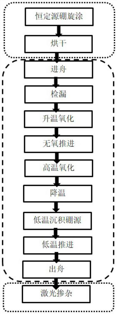
Figure 1 
Figure 2
Abstract
Description
technical field
[0001] The invention relates to the field of solar cell manufacturing, in particular to a boron process suitable for P+ selective emitter cells. Background technique
[0002] As the demand for affordable Internet access intensifies, high-efficiency batteries have become a development trend. Especially today's N-TOPCon batteries are getting more and more popular. However, how to raise the efficiency of N-TOPCon batteries to a higher level has become the focus of research and development. Among them, boron diffusion is widely used in N-type high-efficiency solar cells as an important means of p+ layer doping. The common method is to carry gas boron source into the furnace tube for single boron doping, but for boron selective doping diffusion technology is still blank.
[0003] Moreover, the conventional boron diffusion process is required to form a good ohmic contact with the metal electrode, and the square resistance is low, which leads to high recombinatio...
Examples
Embodiment 1
[0048] A constant source boron diffusion process suitable for P+ selective emitter batteries, the specific process is as follows: use N-type silicon wafers with high minority carrier life, resistivity 0.2-2Ω.cm, double-sided alkali washing for texture;
[0049] (1) Constant source boron spin-coating—use 1-1.5mL of immersion solution to spin on the silicon wafer, and then drop 0.4-0.8ml of boron source to spin on the silicon wafer. The spin coating method can produce a higher square resistance of 120-140ohm, and the uniformity STD<8;
[0050] (2) Drying—on a chain machine at a temperature of 120-200°C and a drying time of 30-60s;
[0051] (3) Entering the boat - the temperature is maintained at 750-850°C, the nitrogen flow rate is 1000-2000sccm, and the time is about 8-15min;
[0052] (4) Leak detection - the flow rate of nitrogen gas is 1000-1500sccm, and the pressure is controlled at 100-200pa;
[0053] (5) Heating Oxidation—The temperature rises to 900-960°C, the nitrogen ...
Embodiment 2
[0063] A constant source boron diffusion process suitable for P+ selective emitter batteries, the specific process is as follows: use N-type silicon wafers with high minority carrier life, resistivity 2-6Ω.cm, double-sided alkali-washed texture;
[0064] (1) Constant source boron spin-coating—use 1.5-2.5mL of immersion solution to spin on the silicon wafer by spin-coating, and then drop 0.3-0.6ml of boron source to spin on the silicon wafer. The spin coating method can produce a higher square resistance of 130-200ohm, and the uniformity STD: 9-10;
[0065] (2) Drying—on a chain machine at a temperature of 180-250°C and a drying time of 40-80s;
[0066] (3) Entering the boat - the temperature is maintained at 750-850°C, the nitrogen flow rate is 1500-2500sccm, and the time is about 6-15min;
[0067] (4) Leak detection - the nitrogen flow rate is 1500-2500sccm, and the pressure is controlled at 100-200pa;
[0068] (5) Heating Oxidation—The temperature rises to 950-1000°C, the ...