
Periodic stripe domain structure of ferroelectric thin film and method for characterizing same
A ferroelectric thin film, periodic technology, applied in circuits, electrical components, electric solid devices, etc., can solve the problem of not conducting more detailed analysis, and achieve the effect of large polarization value and good ferroelectricity
Patent Information
- Authority / Receiving Office
- CN · China
- Patent Type
- Applications(China)
- Current Assignee / Owner
- Publication Date
- 2019-12-31
Smart Images
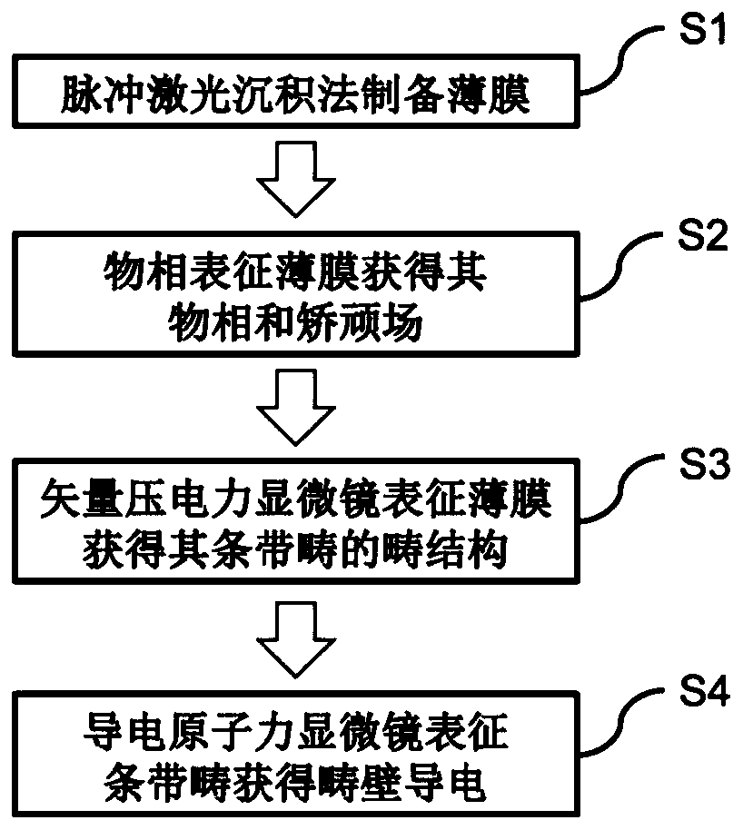
Figure 1 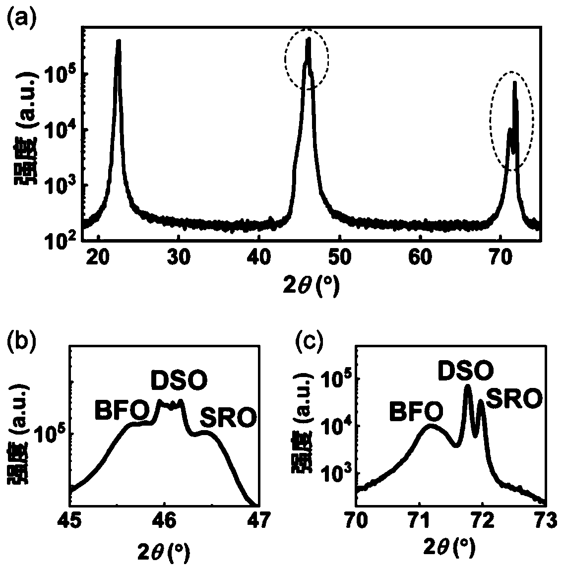
Figure 2 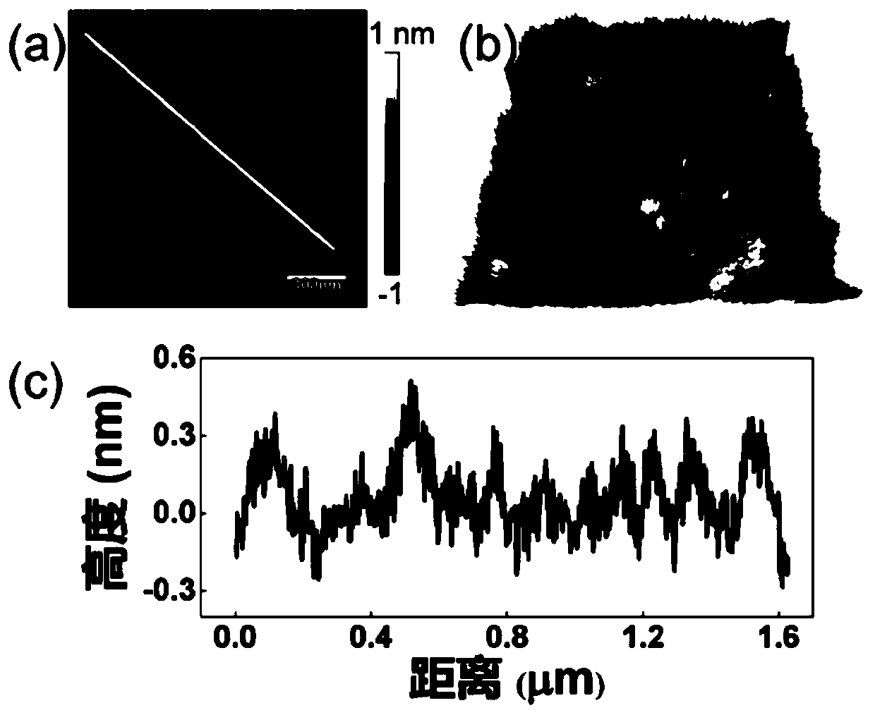
Figure 3
Abstract
Description
technical field
[0001] The invention relates to the technical field of micro-nano characterization, in particular to a periodic striped domain structure of a ferroelectric thin film and a characterization method thereof. Background technique
[0002] Ferroelectric random access memory has the advantages of low energy consumption, fast writing, and much larger erasing times, and is expected to become the next generation of non-volatile memory. Ferroelectric storage requires ferroelectric materials to have a large polarization value and strong piezoelectric response at room temperature, which is conducive to the development and detection of devices based on ferroelectric materials. Among them, bismuth ferrite (BiFeO 3 , abbreviated as BFO) the Curie temperature and Neel temperature of this material are 370 ° C and 830 ° C, respectively, with antiferromagnetic and ferroelectric properties, and the remanent polarization values in the (111) and (001) directions are 100 μC / ...
Examples
Embodiment 1
[0041] like Figure 1-8 as shown, figure 1 It is a schematic flowchart of a periodic striped domain structure of a ferroelectric thin film and a characterization method thereof in the present invention. The operation and implementation parameters of using the PLD method to prepare the BFO thin film have been described in detail in the summary of the invention and the specific implementation manner. Combine below Figure 2-8 , describe this embodiment in detail.
[0042] (1) According to step S2, phase characterization of film samples, please refer to Figure 2-4 .
[0043] figure 2 : X-ray θ-2θ scanning results of thin film samples, (a) is the result of wide range angle scanning, (b) is the enlarged view of 45°-47° range scanning results, where the DSO peak intensity exceeds the range, (c) is Enlarged view of the scanning results in the range of 70°-73°; one is to confirm the structure of the sample as DSO / SRO / BFO; The phase structure is close.
[0044] image 3 : AF...