
Solid-state imaging device, driving method of solid-state imaging device, and electronic device
A camera device, solid-state technology, applied in the direction of TV, color TV, image communication, etc., can solve the problem of inability to read, and achieve the effect of improving cost performance, large dynamic range, and realizing dynamic range.
Patent Information
- Authority / Receiving Office
- CN · China
- Patent Type
- Patents(China)
- Current Assignee / Owner
- Publication Date
- 2022-03-29
Smart Images
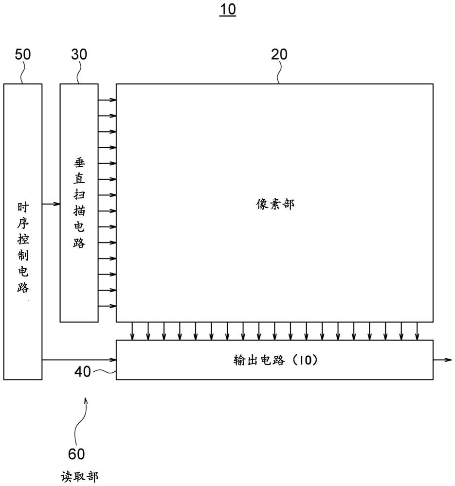
Figure 1 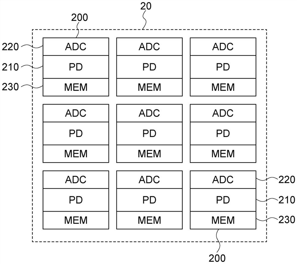
Figure 2 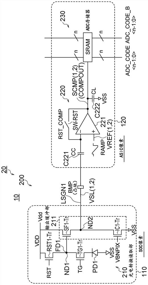
Figure 3
Abstract
Description
technical field
[0001] The present invention relates to a solid-state imaging device, a driving method of the solid-state imaging device, and electronic equipment. Background technique
[0002] A Complementary Metal Oxide Semiconductor (CMOS) image sensor has been put into practical use as a solid-state imaging device (image sensor) using a photoelectric conversion element that detects light and generates charges.
[0003] CMOS image sensors are widely used as part of various electronic devices such as digital cameras, video cameras, surveillance cameras, medical endoscopes, personal computers (PCs), and portable terminal devices (mobile devices) such as mobile phones.
[0004] The CMOS image sensor has an FD amplifier including a photodiode (photoelectric conversion element) and a floating diffusion layer (FD: Floating Diffusion, floating diffusion layer) in each pixel. The mainstream reading type of the CMOS image sensor is column-parallel output type, that is, select a c...
Examples
no. 1 approach
[0073] figure 1 It is a block diagram showing a configuration example of the solid-state imaging device according to the first embodiment of the present invention.
[0074] In the present embodiment, the solid-state imaging device 10 is constituted by, for example, a CMOS image sensor including digital pixels (Digital Pixels) as pixels.
[0075] Such as figure 1 As shown, this solid-state imaging device 10 includes a pixel unit 20 as an imaging unit, a vertical scanning circuit (row scanning circuit) 30 , an output circuit 40 , and a timing control circuit 50 as main constituent elements.
[0076] Among these components, for example, the vertical scanning circuit 30 , the output circuit 40 , and the timing control circuit 50 constitute a pixel signal reading unit 60 .
[0077] In the first embodiment, the solid-state imaging device 10 includes, as digital pixels, a photoelectric conversion reading unit, an AD (analog-to-digital) conversion unit, and a memory unit in the pixe...
no. 2 approach
[0340] Figure 20 It is a circuit diagram showing a configuration example of an SRAM as an ADC memory according to the second embodiment of the present invention.
[0341] The difference between the solid-state imaging device 10A of the second embodiment and the solid-state imaging device 10 of the first embodiment is as follows.
[0342] In the solid-state imaging device 10A of the second embodiment, the SRAM 231A includes a first back-to-back inverter BINV1, a second back-to-back inverter BINV2, a first access transistor AT1, and a second access transistor AT2 to form a bit cell BC, A plurality of bit cells BC are connected in parallel between a virtual power supply node VPN and a virtual ground (reference potential) node VGN.
[0343] That is, it is possible to group several bit cells and perform power gating simultaneously with a group of power gating circuits. This structure can reduce the number of necessary power gate control transistors, further reducing the pixel pi...
no. 3 approach
[0346] Figure 21 It is a circuit diagram showing a configuration example of an SRAM as an ADC memory according to the third embodiment of the present invention.
[0347] The difference between the solid-state imaging device 10B of the third embodiment and the solid-state imaging device 10 of the first embodiment is as follows.
[0348] In the solid-state imaging device 10B of the third embodiment, the SRAM 231B is configured in such a way that write drivers 232B and 232U are arranged at both ends of the bit lines in order to effectively reduce the parasitic resistance of the bit lines BL and BL_B. Both ends drive the SRAM bit cell.
[0349] It is important to reduce the parasitic resistance of the bit lines BL, BL_B. However, the IR drop is caused by the current from the bit cell BC flowing through the parasitic resistance, so including a more powerful write driver doesn't help.
[0350] In order to ensure a proper write operation, not only reducing the current from the bi...