
Low-capacitance high-power transient voltage suppressor and manufacturing method thereof
A technology of transient voltage suppression and manufacturing method, which is applied in the manufacture of semiconductor/solid-state devices, electric solid-state devices, circuits, etc., can solve the problems of increased parasitic capacitance, inability to meet high-speed signal port transmission, data loss, etc., and achieve high reliability. performance, avoiding the risk of potential failure
Patent Information
- Authority / Receiving Office
- CN · China
- Patent Type
- Applications(China)
- Current Assignee / Owner
- Publication Date
- 2020-07-24
Smart Images
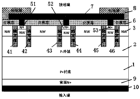
Figure 1 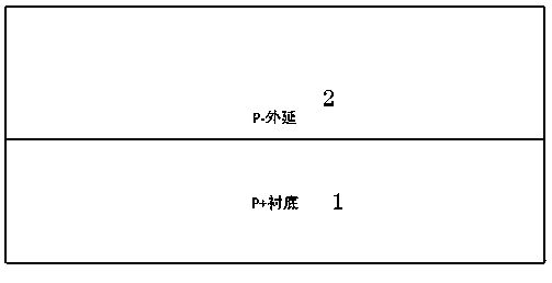
Figure 2 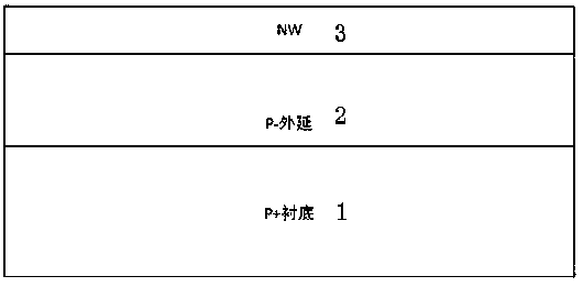
Figure 3
Abstract
Description
technical field
[0001] The invention belongs to the field of semiconductor protection devices, in particular to a low-capacity transient voltage suppressor applied to a signal port and a manufacturing method thereof. Background technique
[0002] Transient Voltage Suppressors (TVS for short) is a commonly used protection device, which has extremely fast response speed and considerable surge discharge capability. When it is subjected to a momentary high-energy surge or electrostatic shock, TVS can change the impedance value between the two ends from high impedance to low impedance at a very high speed, so as to discharge a momentary large current, and at the same time reduce the voltage across the two ends. It is clamped at a small value to protect the downstream circuit chip from the impact of transient high-voltage surge pulses, so TVS is an essential protection device.
[0003] When the transient voltage suppressor is applied to various signal transmission ports, on the o...
Examples
Embodiment 1
[0070] A low capacitance high power transient voltage suppressor such as figure 1 with 8 As shown, the present invention grows P- epitaxial layer 2 on the front of P+ substrate 1 by P+ substrate; N lightly doped NW region 3 is grown on the surface of P- epitaxial layer, and NW region 3 is formed by isolation grooves one, two, three, Four, five, and six 41, 42, 43, 44, 45, and 46 constitute three pairs of ablation grooves, the groove depth is greater than the thickness of the NW layer, and the NW in each pair of isolation grooves is doped with N-type heavy doping to form an N+ region 1, 2, 3 51, 52, 53, there is a dielectric layer 6 on the upper surface of the silicon wafer composed of NW, N+ and isolation grooves, and the front metal layer 7 is connected to the upper surface of the N+ region 1, 2, 3 51, 52, 53 Metal leads, connected to the front metal layer 7, with a passivation layer 8 on the upper surface, forming a front metal window, used for the grounding terminal in the...
Embodiment 2
[0096] In this embodiment, a low-capacitance high-power transient voltage suppressor, such as Figure 9As shown, the others are the same as in Embodiment 1, except that the photolithography plate is omitted before the front N+ layer 5 with the same or similar chip area is injected into the front side, and the entire surface is directly implanted on the upper surface of the silicon wafer, so that the performance is not affected. Next, the manufacturing cost is reduced.
[0097] On the back of the substrate, a large-area N+ / P+ junction reverse-biased diode T1 with the same area as the entire chip is formed by doping, and three small-junction area P+ substrate / P- epitaxy / NW / A diode series structure composed of N+.
Embodiment 3
[0099] In this embodiment, a low-capacitance high-power transient voltage suppressor, such as Figure 10 As shown, the others are the same as in Embodiment 1, except that shallow grooves 1 and 2 111 and 112 on the back are added, and the depth of the grooves is greater than that of the N+ junction on the back.
[0100] On the back of the P+ substrate, the back N+ layer is formed by doping to form a large-area N+ / P+ junction reverse-biased diode T1 that is similar to the entire chip area, and three small junction areas that are limited in each group of isolation grooves P+ substrate / P -Diode series structure composed of epitaxial / NW / N+.