
A kind of electroplating system and method for bga area in pcb board
A PCB board and area technology, applied to the electroplating system and field of the BGA area in the PCB board, can solve the problems of low signal transmission performance and poor uniformity in the PCB board
Patent Information
- Authority / Receiving Office
- CN · China
- Patent Type
- Patents(China)
- Current Assignee / Owner
- Publication Date
- 2021-11-23
Smart Images
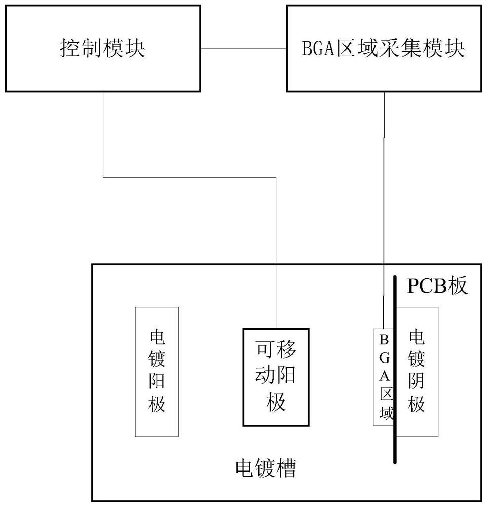
Figure 1 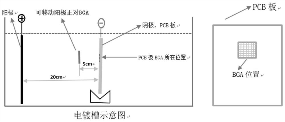
Figure 2 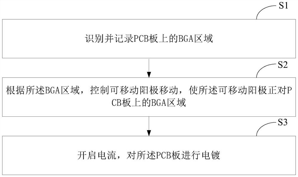
Figure 3
Abstract
Description
technical field
[0001] The present application relates to the technical field of PCB (Printed Circuit Board, printed circuit board) board manufacturing, in particular to an electroplating system and method for a BGA (Ball Grid Array Package, ball grid array package) area in a PCB board. Background technique
[0002] The PCB board of the server is used to install the CPU, and there are many densely arrayed small holes, collectively referred to as BGA holes. During the electroplating process of the PCB board, due to the current rush effect, the copper plating at these dense BGA hole positions is relatively thin, for example: the copper plating thickness at other positions is 30 μm, while the copper plating thickness at the BGA position is 10 μm. The copper plating at the dense BGA hole position is relatively thin, which will affect the performance of the entire PCB board. Therefore, how to electroplate the BGA area in the PCB to ensure the overall performance of the PCB is an...
Examples
Embodiment 1
[0041] see figure 1 , figure 1 It is a schematic structural diagram of an electroplating system for a BGA area in a PCB board provided by an embodiment of the present application. Depend on figure 1 It can be seen that the electroplating system in the BGA area of the PCB board in this embodiment mainly includes four parts: an electroplating tank, a BGA area acquisition module, a control module and a movable anode.
[0042]Among them, the electroplating tank is provided with an electroplating anode and an electroplating cathode, the electroplating anode is parallel to the electroplating cathode, the PCB board is placed on the electroplating cathode, the movable anode is parallel to the electroplating cathode, and the horizontal distance between the movable anode and the electroplating cathode is less than the electroplating cathode. The horizontal distance between the anode and the plating cathode. The BGA area acquisition module is used to identify and record the BGA area...
Embodiment 2
[0052] exist figure 1 with figure 2 On the basis of the illustrated embodiment see image 3 , image 3 It is a schematic flowchart of a method for electroplating a BGA area in a PCB board provided by an embodiment of the present application. Depend on image 3 It can be seen that the electroplating method of the BGA area in the PCB board of this embodiment mainly includes the following processes:
[0053] S1: Identify and record the BGA area on the PCB. Specifically, step S1 includes:
[0054] S11: Collect the arrangement of BGA holes on the PCB, and the BGA holes are used to install the CPU.
[0055] In this embodiment, the camera can be used to capture the layout of the BGA holes on the PCB.
[0056] S12: Identify the BGA area according to the arrangement of the collected BGA holes.
[0057] Specifically, step S12 includes the following processes:
[0058] S121 : According to the arrangement of the collected BGA holes, it is judged whether the number of holes in th...