

Separated gate CSTBT with self-biased PMOS and manufacturing method thereof
A separation gate and self-biasing technology is applied in the field of separation gate CSTBT and its production, which can solve the problems of CSTBT device breakdown voltage drop, device saturation current density increase, and short-circuit safe working area deterioration, etc., so as to improve device reliability. , reduce saturation current, improve the effect of clamping effect
Patent Information
- Authority / Receiving Office
- CN · China
- Patent Type
- Applications(China)
- Current Assignee / Owner
- Publication Date
- 2021-12-24
Smart Images
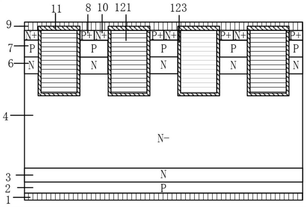
Figure 1 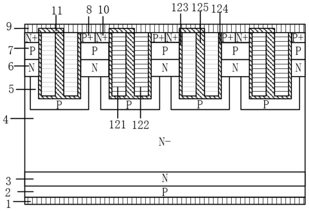
Figure 2 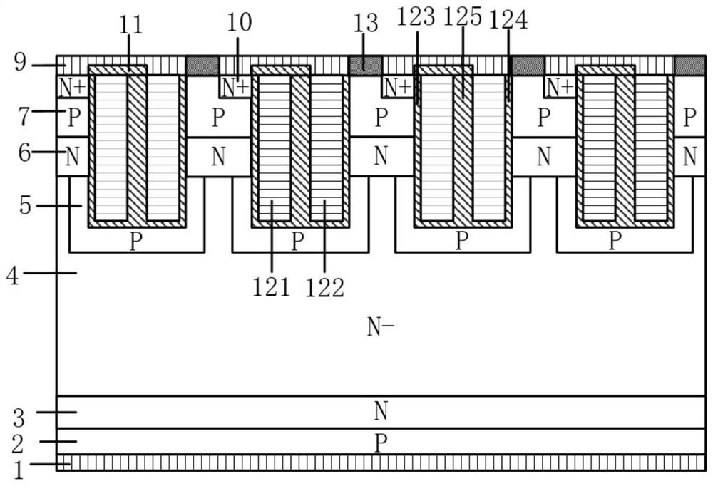
Figure 3
Abstract
Description
technical field
[0001] The invention belongs to the technical field of power semiconductor devices, and in particular relates to a split gate CSTBT with self-biased PMOS and a manufacturing method thereof. Background technique
[0002] Insulated gate bipolar transistor (IGBT), as one of the core electronic components in modern power electronic circuits, is widely used in various fields such as transportation, communication, household appliances, and aerospace. The insulated gate bipolar transistor is a new type of power electronic device composed of an insulated field effect transistor (MOSFET) and a bipolar junction transistor (BJT), which can be equivalent to a MOSFET driven by a bipolar junction transistor. The IGBT combines the MOSFET structure and the working mechanism of the bipolar junction transistor. It not only has the advantages of easy driving, low input impedance, and fast switching speed of the MOSFET, but also has the advantages of large on-state current densi...
Examples
Embodiment Construction
[0057] The principles and features of the present invention are described below in conjunction with the accompanying drawings. The specific embodiments of the present invention are illustrated by taking an IGBT with a voltage level of 1200V as an example. The examples are only used to explain the present invention, not to limit the scope of the present invention.
[0058] Such as figure 2 As shown, a self-biased PMOS split-gate CSTBT provided in Embodiment 1 of the present invention has a cell structure including back collector metal 1, P-type collector region 2, and N-type field stacked sequentially from bottom to top. Blocking layer 3 and N-drift region 4; the upper layer of the N-drift region 4 has N-type charge storage layers 6 and trench structures alternately arranged, and the depth of the lower surface of the trench structure is greater than that of the N-type charge storage layer 6 the junction depth of the lower surface;
[0059] The upper surface of the N-type char...