
Semiconductor structure and forming method thereof
A semiconductor and wet etching technology, which is applied in semiconductor devices, semiconductor/solid-state device manufacturing, transistors, etc., can solve the problems of device reliability decline, semiconductor structure performance reduction, fin damage, etc., to reduce consumption and improve Fin width uniformity and height uniformity, effect of improving performance
Patent Information
- Authority / Receiving Office
- CN · China
- Current Assignee / Owner
- Publication Date
- 2022-07-29
Smart Images
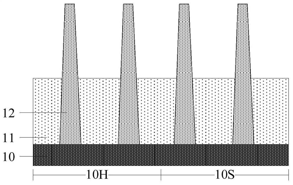
Figure 1 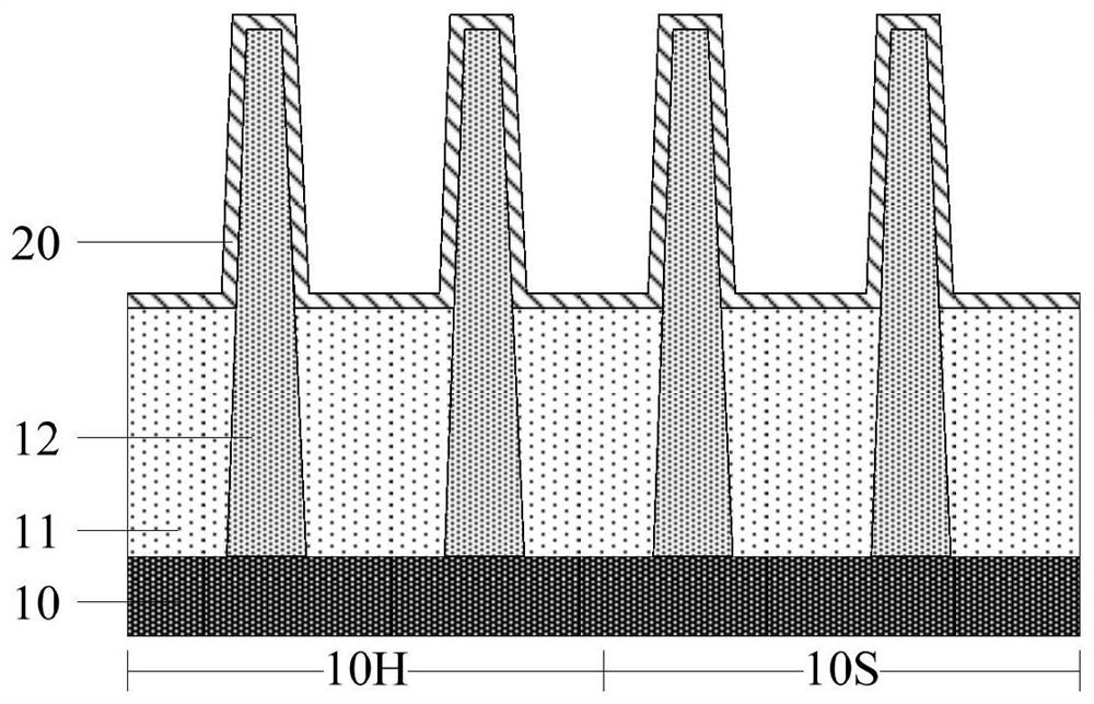
Figure 2 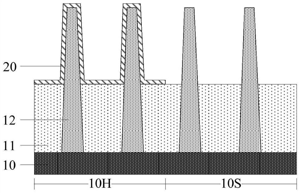
Figure 3
Abstract
Description
technical field
[0001] Embodiments of the present invention relate to the field of semiconductor manufacturing, and in particular, to a semiconductor structure and a method for forming the same. Background technique
[0002] As the integration level of semiconductor devices becomes higher and higher, the voltage and current required for the operation of semiconductor devices continue to decrease, and the switching speed of transistors is also accelerated, and the requirements for all aspects of semiconductor technology are greatly increased. A gate last process is formed, that is, a dummy gate structure is formed first, source / drain implantation and high temperature annealing processes are performed, the dummy gate structure is removed, a gate oxide layer is deposited, and finally a gate structure is formed.
[0003] The gate oxide layer is an important structure in a semiconductor device such as a MOSFET (Field Effect Transistor), and if there are defects on the gate oxide ...
Examples
Embodiment Construction
[0035] The performance of the current semiconductor structure still needs to be improved. Now combined with a method of forming a semiconductor structure to analyze the reasons why its performance still needs to be improved.
[0036] refer to Figure 1 to Figure 4 , a schematic diagram of the structure corresponding to each step in a method for forming a semiconductor structure is shown.
[0037] refer to figure 1 , providing a base, including a substrate 10 and a fin portion 12 protruding from the substrate 10 , an isolation layer 11 is formed on the substrate 10 exposed by the fin portion 12 , and the isolation layer 11 covers the fin portion 12 part of the sidewall, the substrate includes a first region 10H for forming a first device and a second region 10S for forming a second device, wherein the operating voltage of the first device is greater than that of the second device Operating Voltage.
[0038] refer to figure 2 , forming a second gate oxide layer 20 conforma...