
Waveguide structure and method of manufacturing the same
Patent Information
- Authority / Receiving Office
- US · United States
- Current Assignee / Owner
- Publication Date
- 2005-04-28
Smart Images
Figure 1 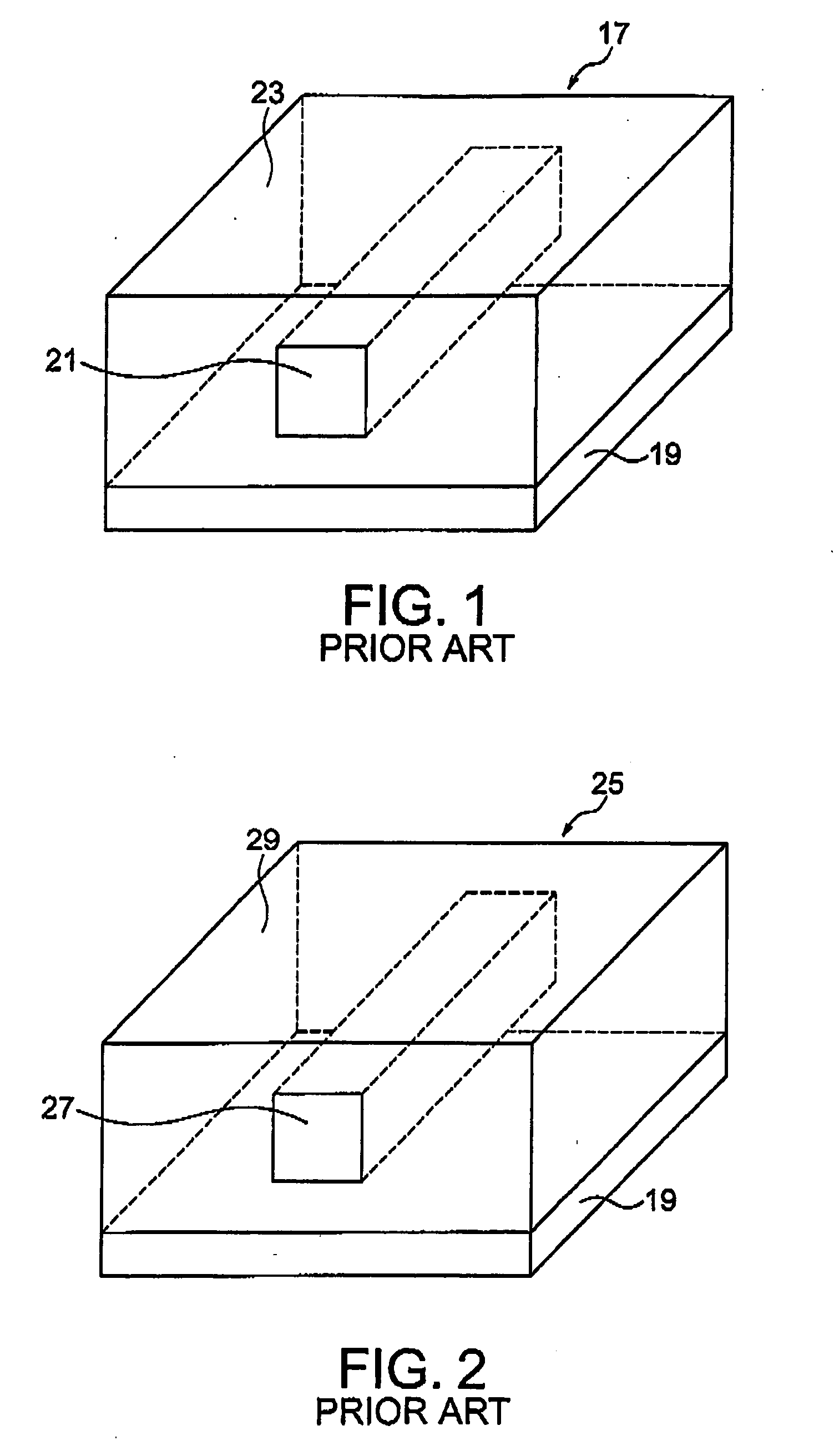
Figure 2 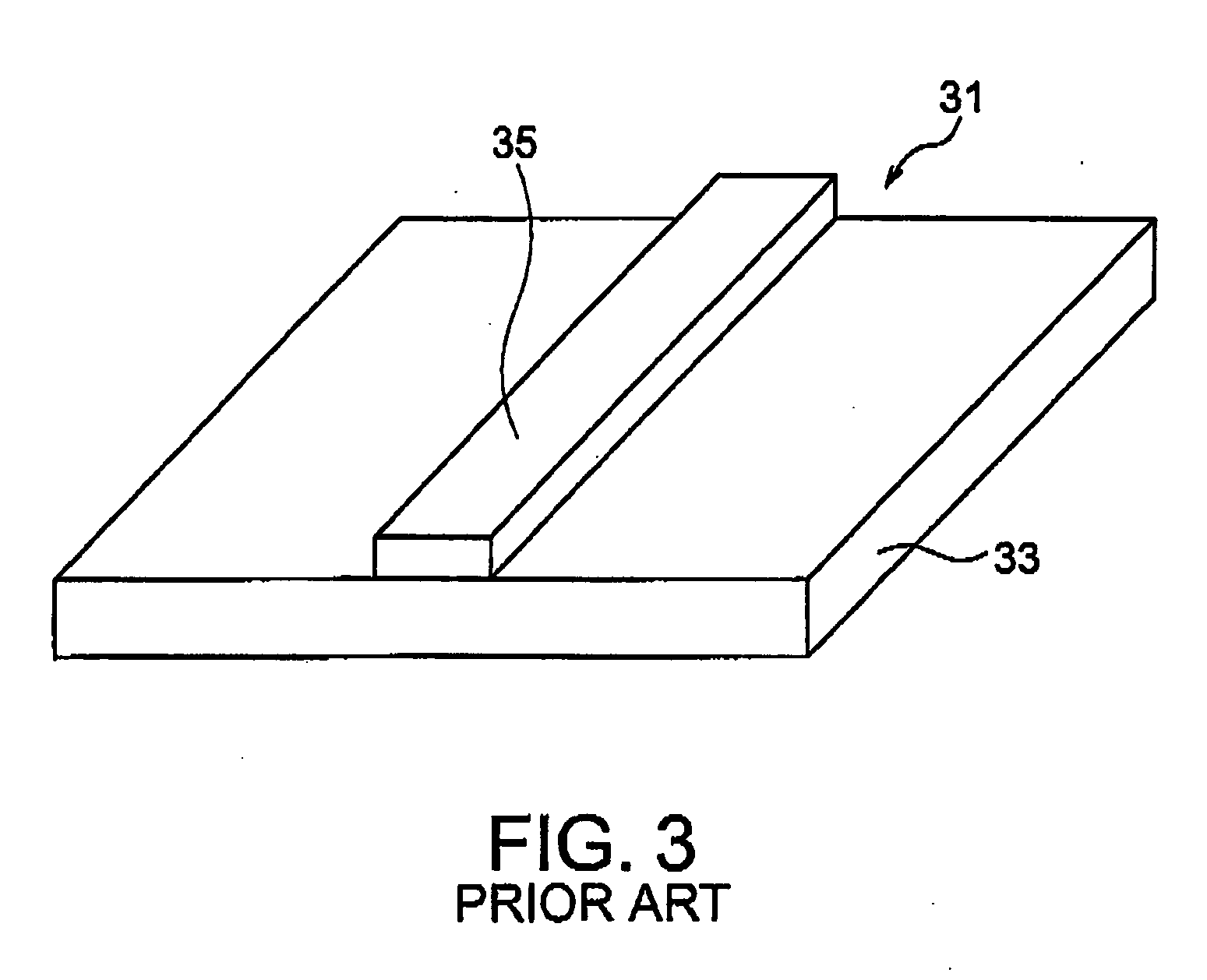
Figure 3
Abstract
Description
BACKGROUND OF THE INVENTION
[0001] (1) Field of the Invention
[0002] The present invention relates to a new structure and manufacturing method of a waveguide, and more particularly, to a structure and manufacturing method of a waveguide that can be used for an optical integrated circuit.
[0003] (2) Description of the Related Art
[0004] Conventionally, waveguide structures used for optical integrated circuits include, (i) silica-based waveguides, as shown in Japanese Laid-Open Patent Publication (JP-A) No. 2002-14242A and Japanese Laid-Open Patent Publication (JP-A) No. 2001-133648A (hereinafter referred to respectively as Reference 1 and Reference 2), (ii) polymer-based waveguides, as shown in Japanese Laid-Open Patent Publication (JP-A) No. H10-3013A (hereinafter referred to as Reference 3), and (iii) Si-wire waveguides, as shown in Japanese Laid-Open Patent Publication (JP-A No. 2002-323633 (hereinafter referred to as Reference 4).
[0005] The above-mentioned (i) silica-based waveg...
Examples
Embodiment Construction
[0039] For a better understanding of the present invention, waveguides according to the related art will be explained using FIGS. 1 to 3 before explaining the embodiments of the present invention.
[0040] With reference to FIG. 1, a silica-based waveguide 17 of (i) has a core 21 and a cladding layer 23 made of silica glass (SiO2) formed on a substrate 19. By doping the core 21 with Ge or the like, a difference is made in refractive index between the core 21 and the cladding layer 23 of about 2 to 5% in order to guide light. It is widely used for a planer lightwave circuit (PLC). An AWG, which is used widely for communications, is achieved using this technique.
[0041] With reference to FIG. 2, a polymer-based waveguide 25 in (ii) has a core 27 and a cladding layer 29, both made of a polymer material such as PMMA or polyimide: a minute difference is made in refractive index between the material forming the core 27 and the material forming the cladding layer 29 in order to guide light. ...