
DC-DC regulator with switching frequency responsive to load
Patent Information
- Authority / Receiving Office
- US · United States
- Current Assignee / Owner
- Publication Date
- 2005-08-25
Smart Images
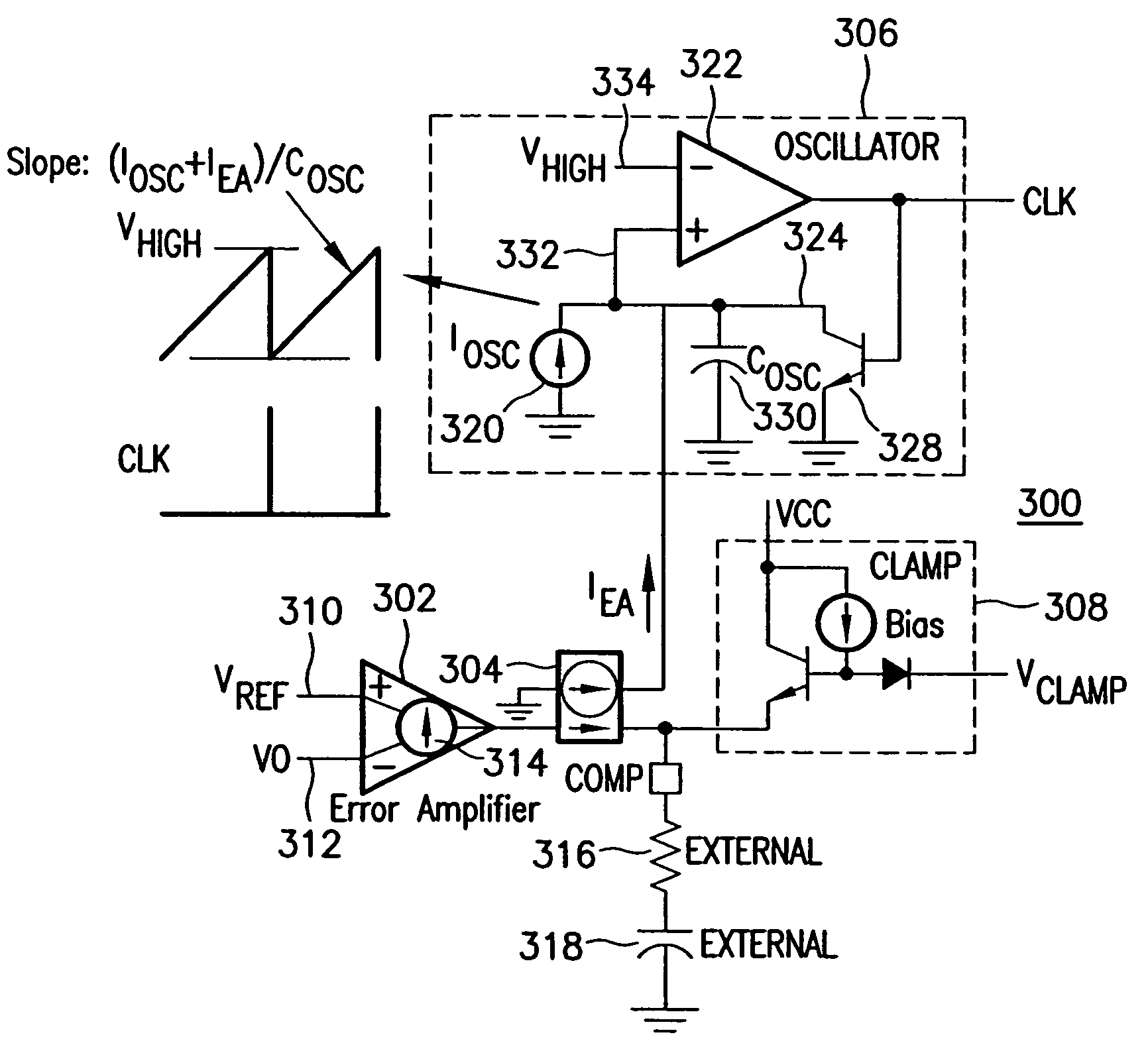
Figure 1 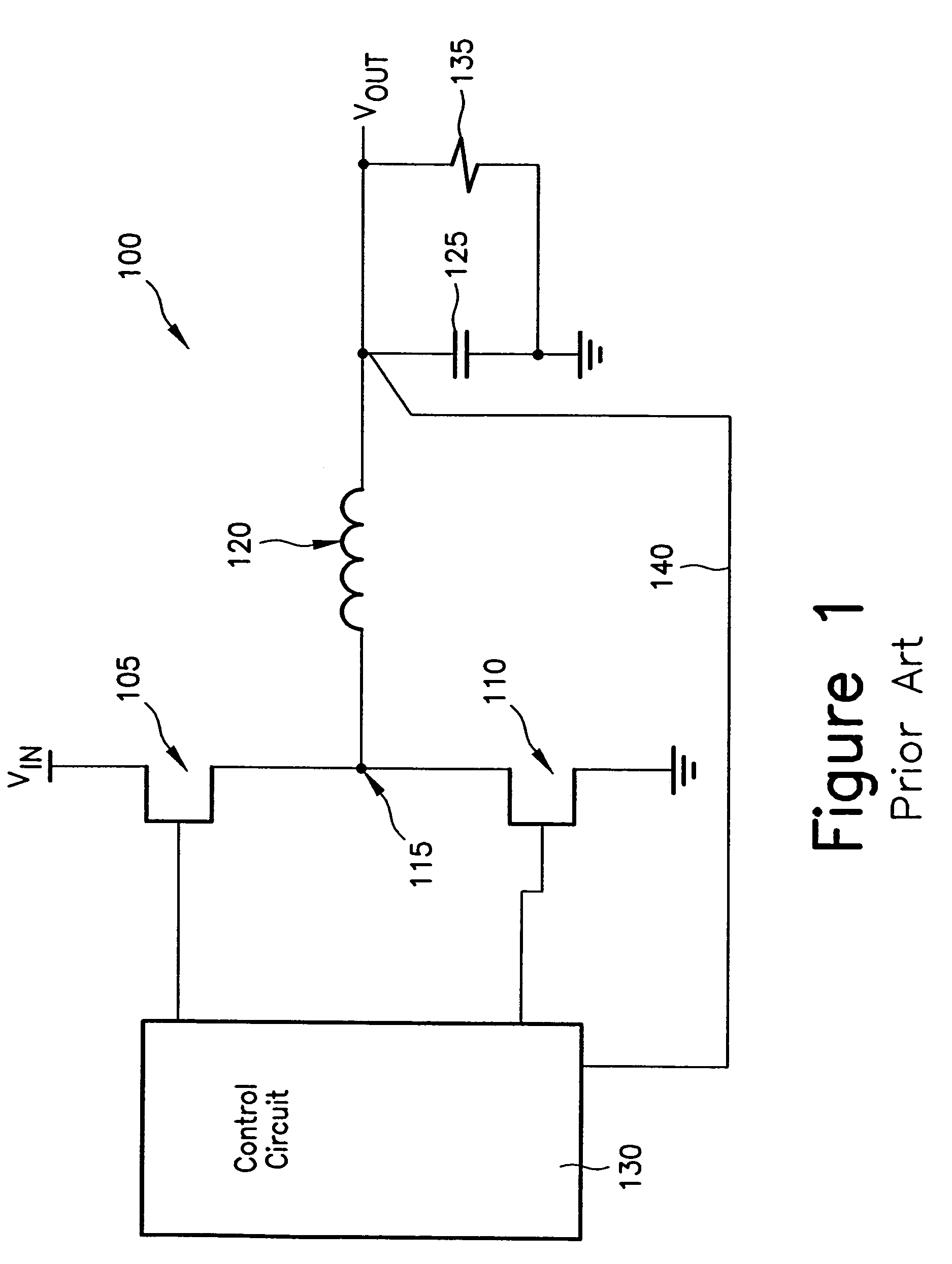
Figure 2 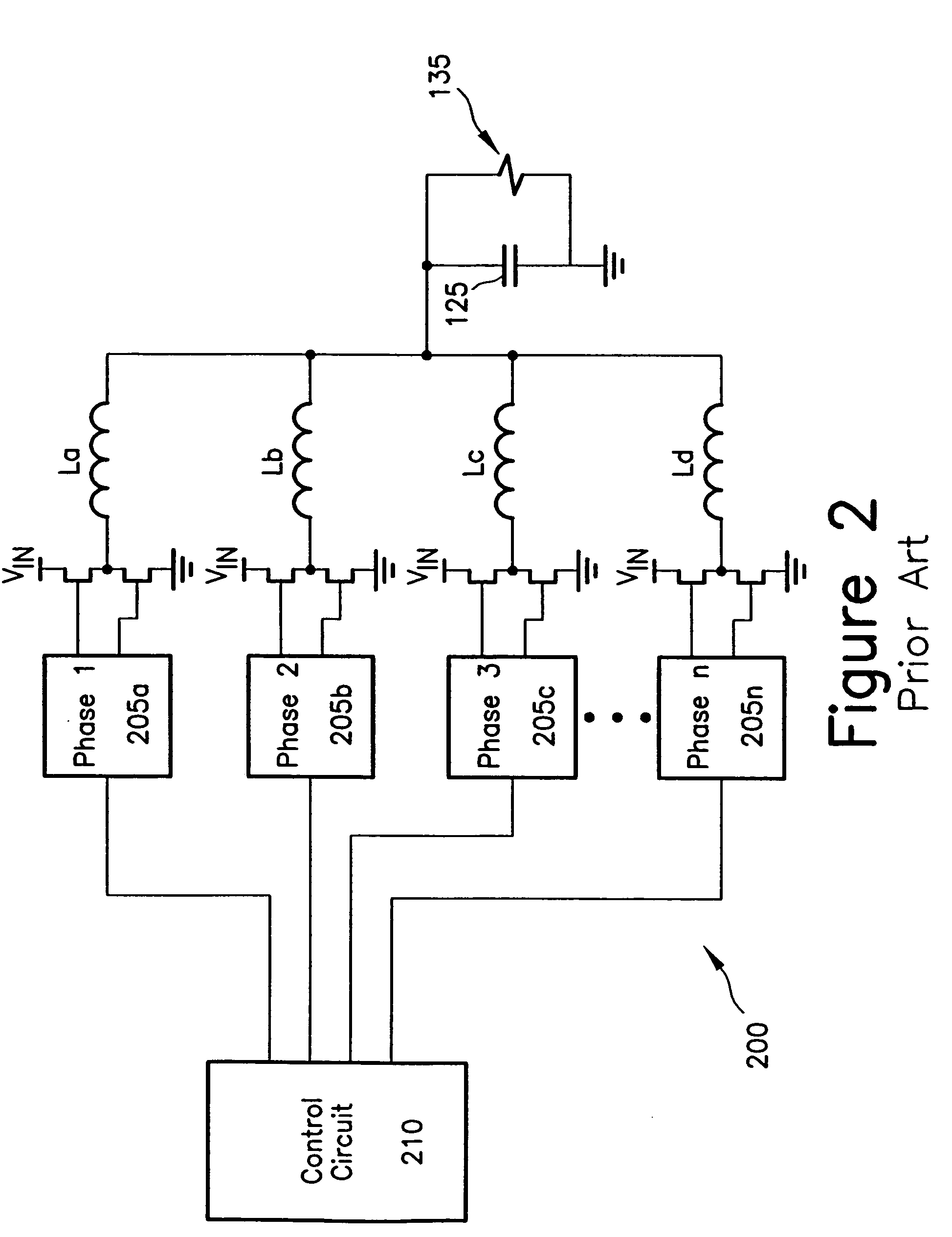
Figure 3
Abstract
Description
RELATED APPLICATION
[0001] The present application is based on and claims the benefit of U.S. Provisional Application No. 60 / 546,119, filed on Feb. 19, 2004, entitled DC-DC REGULATOR WITH SWITCHING FREQUENCY RESPONSIVE TO LOAD, the entire contents of which are expressly incorporated herein by reference.FIELD OF THE INVENTION
[0002] The present invention relates to switch mode power supplies in which the conventional pulse width modulation (PWM) control of the switching devices is modified to vary the switching frequency so that for light loads, the drive frequency is decreased, and for step load increases, the drive frequency is increased. BACKGROUND OF THE INVENTION
[0003] Switched power supplies have numerous applications in electronic devices and motor drives, and several basic types are well known to those skilled in the art. For purposes of illustration, the invention will be described in the context of a conventional DC-to-DC buck converter that accepts a DC input voltage and ...
Examples
Embodiment Construction
[0032] Referring now to FIG. 3, there is shown a first embodiment of a variable frequency gate drive oscillator according to the invention, generally designated at 300. This is intended to be implemented using standard integrated circuit fabrication techniques and circuit designs, and therefore the description will be limited to the system architecture and functionality. Those skilled in the art will readily understand how the invention is to be implemented from the following description using any suitable circuit design.
[0033] Frequency controller 300 includes an error amplifier 302, a current mirroring circuit 304, a variable frequency oscillator 306, and a clamping circuit 308. Error amplifier 302 is a transconductance amplifier which receives a reference signal VREF at an input 310, and an error signal VO at a second input 312, the latter representing a feedback signal from the power supply regulation loop 140 (see FIG. 1). A load circuit for error amplifier 302 comprised of a ...