
Semiconductor radiation detector and radiation detection apparatus
Patent Information
- Authority / Receiving Office
- US · United States
- Current Assignee / Owner
- Publication Date
- 2006-03-30
- Estimated Expiration
- Not applicable · inactive patent
Smart Images
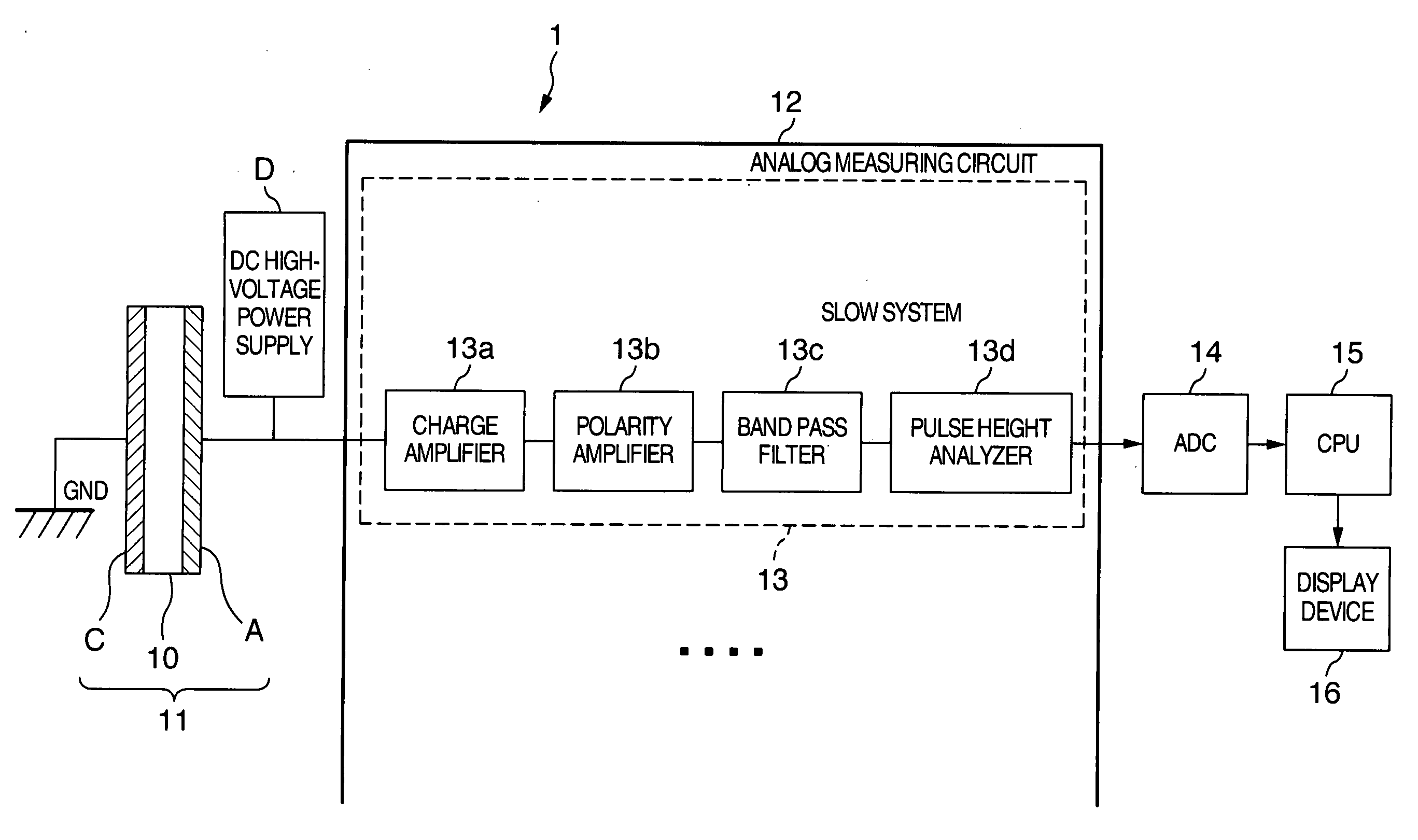
Figure 1 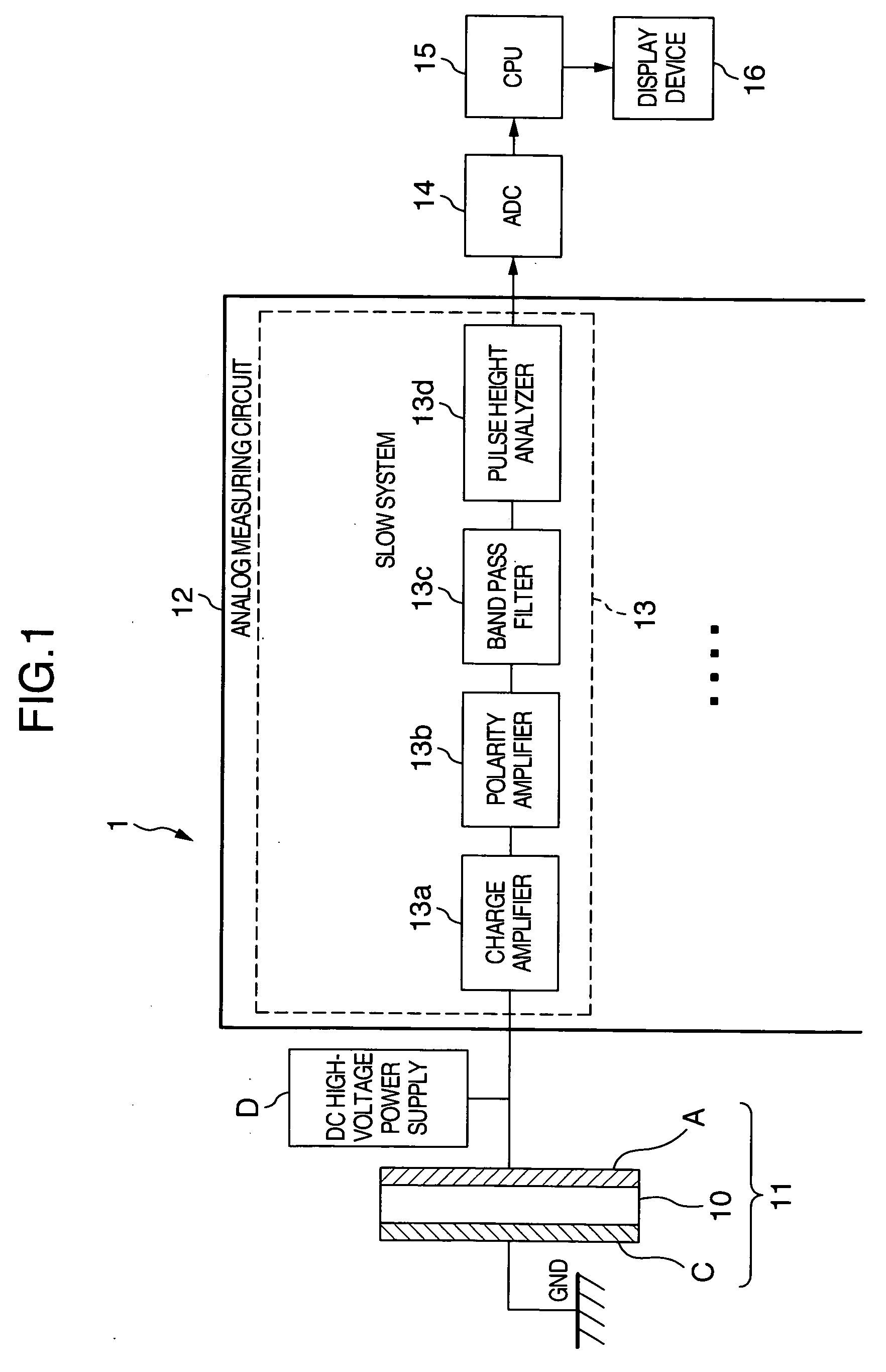
Figure 2 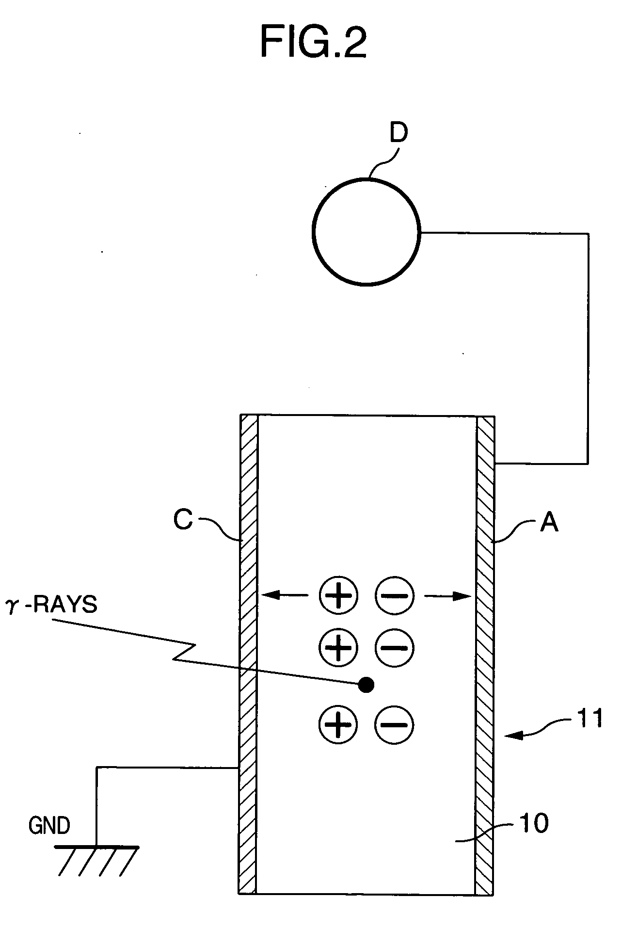
Figure 3
Abstract
Description
BACKGROUND OF THE INVENTION
[0001] The present invention relates to a semiconductor radiation detector and radiation detection apparatus.
[0002] Conventionally, an X-ray machine or radiological imaging apparatus uses a semiconductor radiation detector for detecting radiation such as X-rays which pass through an examinee and γ-rays emitted from a radioactive material given to an examinee. As such a semiconductor radiation detector, one using a semiconductor radiation detection element made of a single crystal of cadmium telluride (CdTe) is known (e.g., see JP-A-2002-168958 (paragraph 0025 and paragraph 0027)). With this semiconductor radiation detector, an attempt is made to increase detection sensitivity of radiation using a single crystal of cadmium telluride with a small content of impurities. Furthermore, JP-A-2002-168958 (paragraph 0025 and paragraph 0027) also describes a semiconductor radiation detection element composed of a polycrystal of thallous bromide (TlBr).
[0003] The ...
Examples
Embodiment Construction
[0017] A radiation detection apparatus which is an embodiment of the present invention will be explained in detail using FIG. 1. The radiation detection apparatus 1 of the present embodiment is an apparatus for detecting radiation such as X-rays and γ-rays, and detection of γ-rays will be explained as an example here. The radiation detection apparatus 1 is provided with a semiconductor radiation detector 11, an analog measuring circuit 12, an analog / digital converter (hereinafter referred to as “ADC”) 14 and a central processing unit (hereinafter simply referred to as “CPU”) 15. Reference character D denotes a DC high-voltage power supply. The analog measuring circuit 12 can also be constructed of an ASIC (application-specific integrated circuit).
[0018] The semiconductor radiation detector 11 is provided with a semiconductor radiation detection element (hereinafter referred to as “semiconductor detection element”) 10 and a cathode electrode C and an anode electrode A attached to th...