

Touch sensor with improved electrode pattern
a technology of electrode pattern and touch sensor, applied in the field of resistive and capacitive touch sensor technology, can solve the problems of increasing the chance of parasitic sourcing and sinking of current on the non-sourcing side, reducing the effective touch region, and reducing the effective touch area. the effect of equipotential line bunching
Patent Information
- Authority / Receiving Office
- US · United States
- Patent Type
- Applications(United States)
- Current Assignee / Owner
- Publication Date
- 2006-06-08
Smart Images
Figure 1 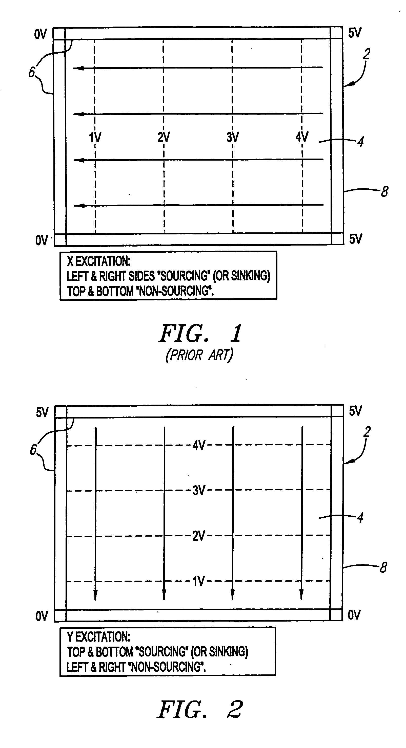
Figure 2 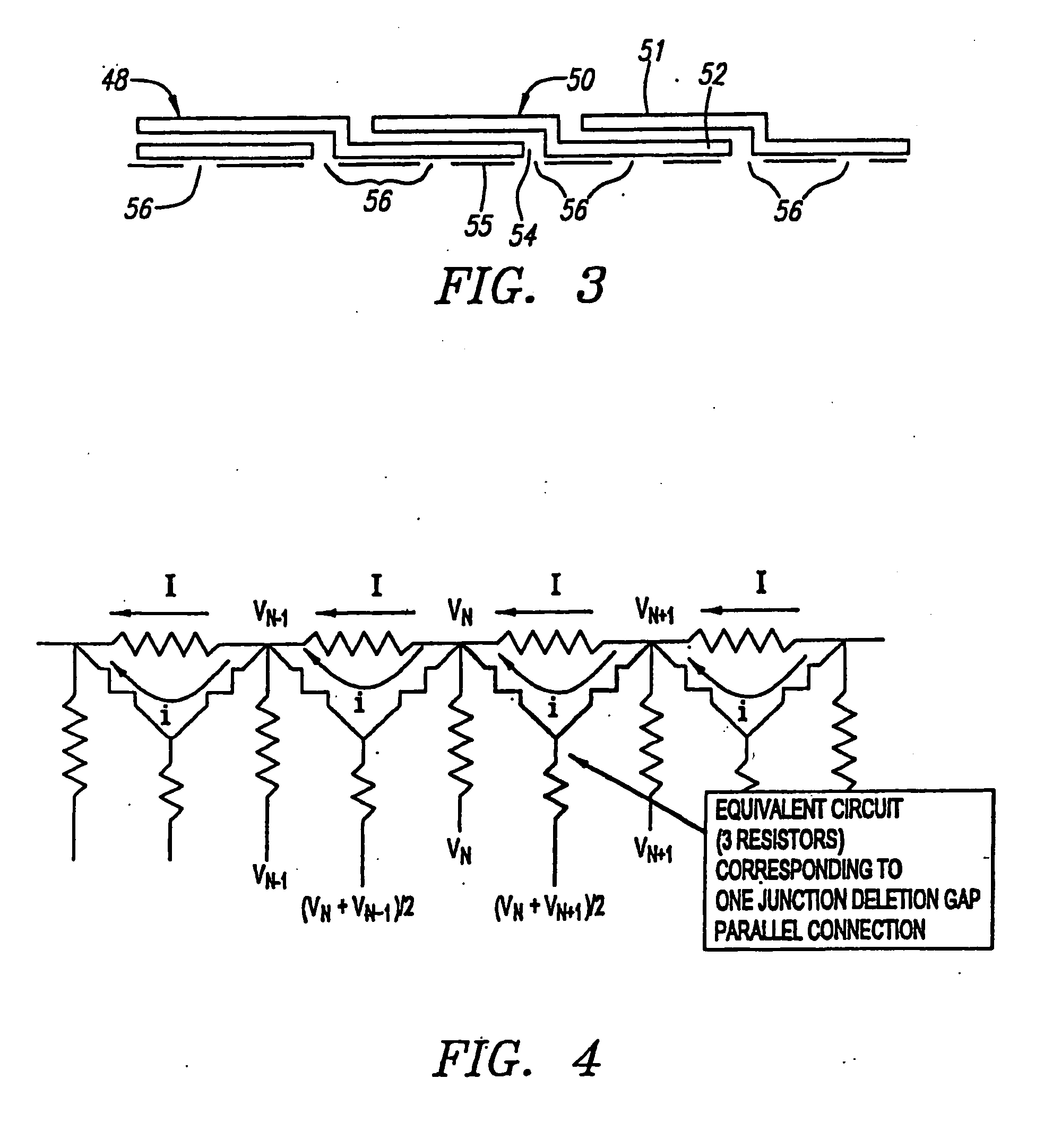
Figure 3
Abstract
Description
RELATED APPLICATIONS
[0001] This application claims the benefit of the filing date of U.S. Provisional Patent Application Ser. No. 60 / 373,022, filed Apr. 16, 2002, and entitled “Touchscreen Having A Series Resistor Chain On The Periphery Of A Touch Area,” which is expressly incorporated herein by reference.FIELD OF THE INVENTION
[0002] The field of the present invention relates to touch sensor technology, and more particularly to resistive and capacitive touch sensor technology. BACKGROUND OF THE INVENTION
[0003] Touch sensors are transparent or opaque input devices for computers and other electronic systems. As the name suggests, touch sensors are activated by touch, either from a user's finger, or a stylus or some other device. Transparent touch sensors, and specifically touchscreens, are generally placed over display devices, such as cathode ray tube (CRT) monitors and liquid crystal displays, to create touch display systems. These systems are increasingly used in commercial appl...
Examples
Embodiment Construction
[0035] Referring to FIG. 7, a resistive touchscreen system 100 constructed in accordance with a preferred embodiment of the present invention is described. The touchscreen system 100 generally comprises a touchscreen 105 (i.e., a touch sensor having a transparent substrate), controller electronics 110, and a display 120. The touchscreen system 100 is typically coupled to a host computer 115. Generally, the controller electronics 110 receives from the touchscreen 105 analog signals carrying touch information. The controller electronics 110 also sends to the touchscreen 105 excitation signals. Specifically, the controller electronics 110 establishes a voltage gradient across the touchscreen 105. The voltages at the point of contact are representative of the position touched. The controller electronics 110 digitizes these voltages and transmits these digitized signals, or touch information in digital form based on these digitized signals, to the host computer 115 for processing.
[0036]...