
Timing analyzer apparatus and timing analysis program recording medium
Patent Information
- Authority / Receiving Office
- US · United States
- Current Assignee / Owner
- Publication Date
- 2007-05-31
- Estimated Expiration
- Not applicable · inactive patent
Smart Images
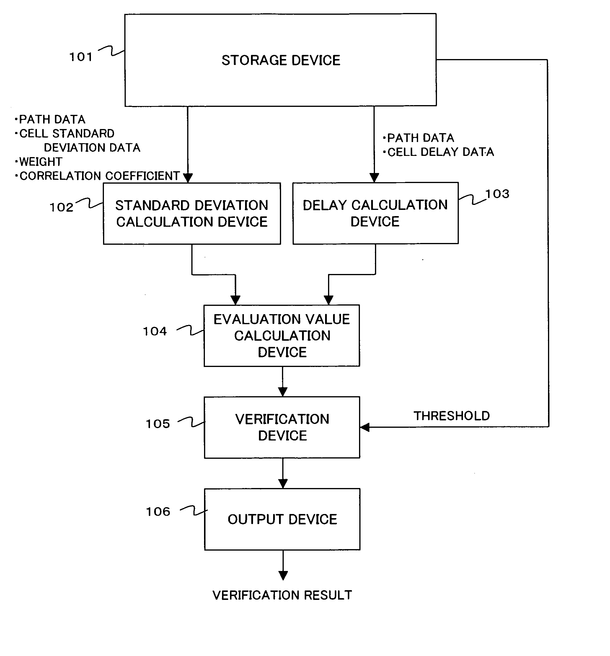
Figure 1 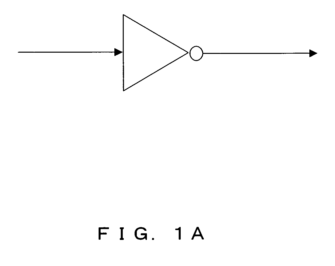
Figure 2 
Figure 3
Abstract
Description
CROSS REFERENCE TO RELATED APPLICATIONS
[0001] This application is based upon and claims the benefit of priority from the prior Japanese Patent Application No. 2005-343640, filed Nov. 29, 2005, the entire contents of which are incorporated herein by this reference. BACKGROUND OF THE INVENTION
[0002] 1. Field of the Invention
[0003] The present invention relates to an apparatus for performing a timing analysis of a circuit in designing a semiconductor integrated circuit and a program thereof.
[0004] 2. Description of the Related Art
[0005] A static timing analysis (STA), used in conventional semiconductor integrated circuit designing, verifies whether a circuit operates or not within a range between the maximum and the minimum delay values with variations, employing delay average value μ and standard deviation σ of a gate circuit, as shown in FIG. 1A. For example, in a case of a 3σ model, the timing verification is performed with in a range of the maximum value μ+3σ and the minimum v...
Examples
Embodiment Construction
[0041] In the following description, details of the preferred embodiment of the present invention are set forth with reference to the drawings.
[0042]FIG. 2 is a diagram showing a principle of first and second timing analyzer apparatuses of the present invention. The timing analyzer apparatus shown in FIG. 2 comprises a storage device 101, a standard deviation calculation device 102, a delay calculation device 103, an evaluation value calculation device 104, a verification device 105, and an output device 106.
[0043] In the first timing analyzer apparatus, the storage device 101 stores a path data indicating a plurality of cells constituting a timing verification target circuit in a semiconductor integrated circuit, delay data and standard deviation data of each cell, a weight for calculating delay of standard deviation of the target circuit, and a threshold of the timing verification.
[0044] The standard deviation calculation device 102, using the path data and standard deviation d...