
Bonding apparatus and method
Patent Information
- Authority / Receiving Office
- US · United States
- Current Assignee / Owner
- Publication Date
- 2007-01-04
- Estimated Expiration
- Not applicable · inactive patent
Smart Images
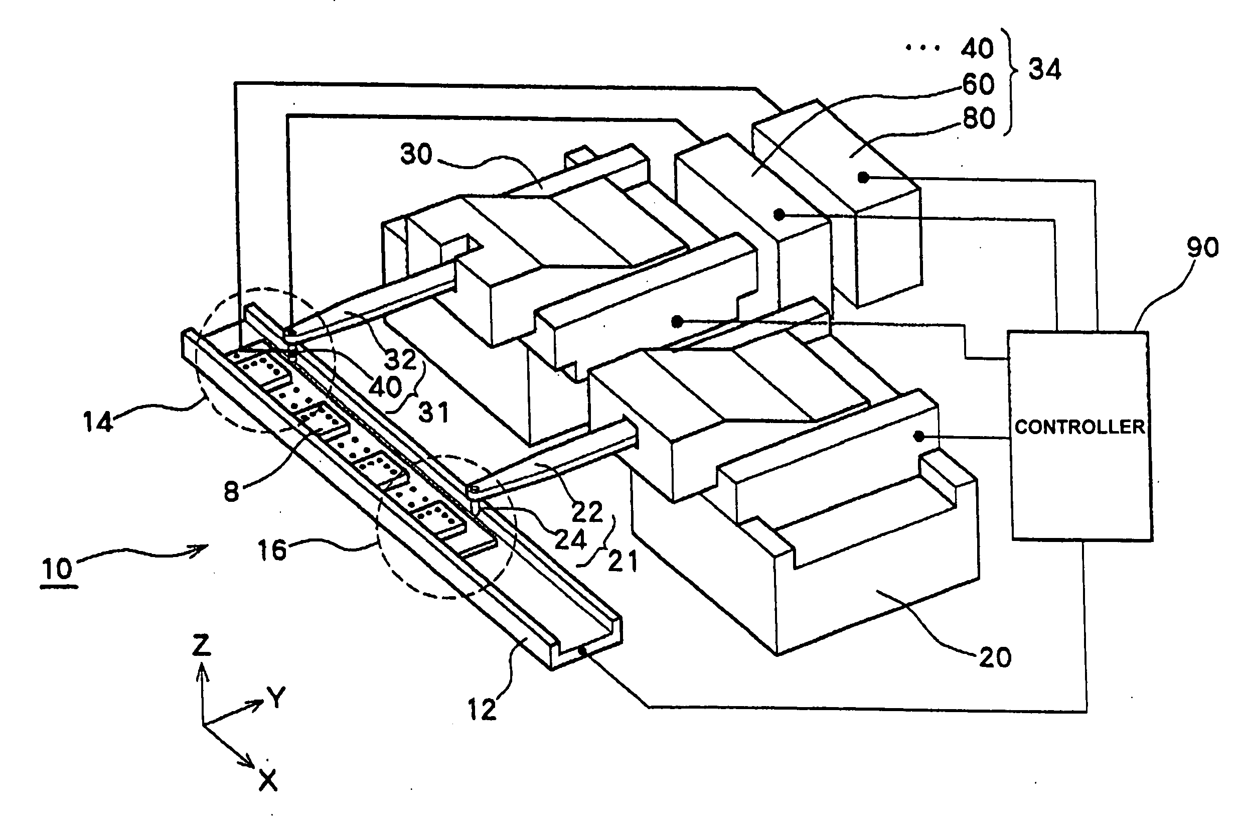
Figure 1 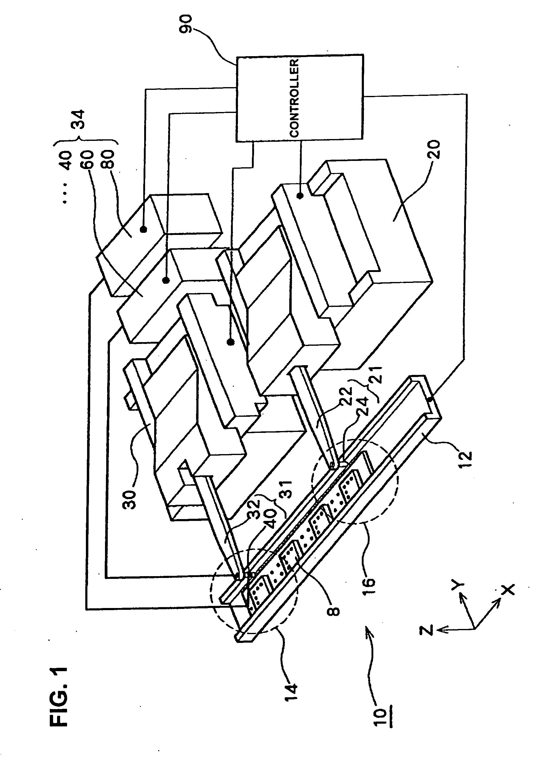
Figure 2 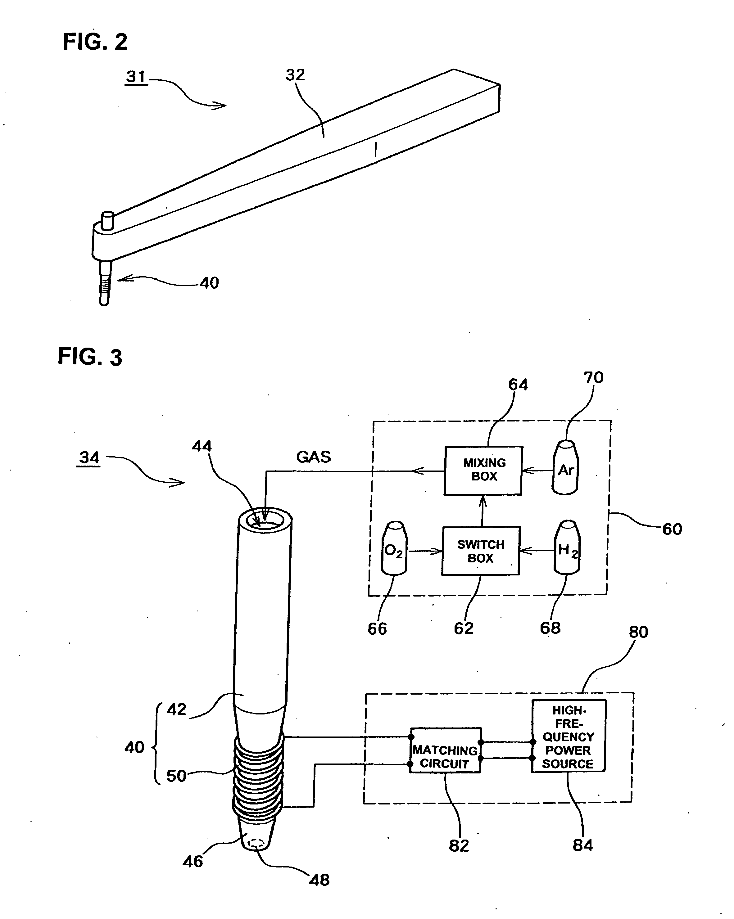
Figure 3
Abstract
Description
BACKGROUND OF THE INVENTION
[0001] The present invention relates to a bonding apparatus and method and more particularly to a bonding apparatus and method for executing a bonding process after performing a surface treatment on a bonding subject on which bonding is executed.
[0002] Bonding apparatuses are generally for making connections between chip electrode units and circuit board lead terminals with fine metal wires. Chip electrode units connected by fine metal wires are sometimes called bonding pads, and circuit board lead terminals are sometimes called bonding leads. When fine metal wires are connected to these elements using ultrasonic connection technology or thermo-compression bonding or the like, it is important to know surface conditions thereof. More specifically, when the surface of either the metal layer of a bonding pad or the metal layer of a bonding lead is contaminated, or foreign matter is present thereon, then it is not possible to obtain a good electrical junctio...
Examples
embodiment 1
[0074]FIG. 1 shows a wire bonding apparatus 10 capable of performing surface treatments and bonding processing. Chips mounted on a substrate are also shown as bonding subjects 8. The wire bonding apparatus 10 has functions for performing a surface treatment by the action of the plasma-state gas, prior to the bonding processing, on a narrow area for performing bonding, specifically on a chip bonding pad and board bonding leads, for a bonding subject 8, and then performing bonding processing.
[0075] The wire bonding apparatus 10 is comprised of a transporter mechanism 12 for holding the bonding subject 8 and transporting it to a prescribed position, a bonding arm 21 having a bonding capillary 24 attached to the tip end of a bonding arm main body 22, a bonding XYZ drive mechanism 20 for movement-driving the bonding arm 21, a plasma arm 31 having a plasma capillary 40 attached to the tip end of a plasma arm main body 32, a surface treatment XYZ drive mechanism 30 for movement-driving th...
embodiment 2
[0105] The microplasma generator 34 shown in FIG. 3 can be applied to a bump bonding apparatus. A bump bonding apparatus is an apparatus for forming metal bumps in flip chip technology. More specifically, such an apparatus uses the principle of wire bonding to a bonding pad on a chip to bond metal wires and make those metal bumps. Thus it might be characterized as equivalent to an ordinary wire bonding process from which the second bonding is eliminated. Accordingly, such an apparatus corresponds to the wire bonding apparatus 10 shown in FIG. 1, in which the bonding subject 8 transported by the transporter mechanism 12 has been made a completed wafer on which completed LSIs are arrayed.
[0106] When the bonding subject 8 is a completed wafer, in the surface treatment stage 14, bonding pads 5 are surface-treated, respectively, for a plurality of completed LSIs. Then, when surface treatment on all of the bonding pads has been completed for one completed wafer, the bonding subject 8 is ...
embodiment 3
[0111] The microplasma generator 34 shown in FIG. 3 can be applied to a flip chip bonding apparatus. A flip chip bonding apparatus is an apparatus for placing a chip on which a bump is formed as shown in FIGS. 7(a) through 7(c) face down on a circuit board. Accordingly, in such cases, the bump 3 on the chip 6 and the bonding lead 4 connected. Furthermore, the chip is inverted in order to place it face down, and the bonding tool for effecting facedown bonding is not a bonding capillary but a collet for holding the chip placed face down. Thus the specific configuration of a flip chip bonding apparatus differs considerably from that of a wire bonding apparatus.
[0112] There are two stages in applying the microplasma generator 34 in a flip chip bonding apparatus, namely when surface-treating the chip bump 3, before inverting the chip and holding it with the collet, and when surface-treating the bonding lead 4 before effecting facedown bonding with the collet
[0113] FIGS. 8(a) through 8(...