
Method of fabricating substrate with embedded component therein
Patent Information
- Authority / Receiving Office
- US · United States
- Current Assignee / Owner
- Publication Date
- 2007-08-16
Smart Images
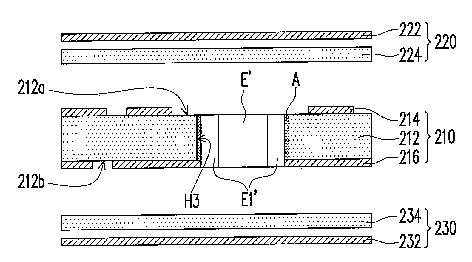
Figure 1 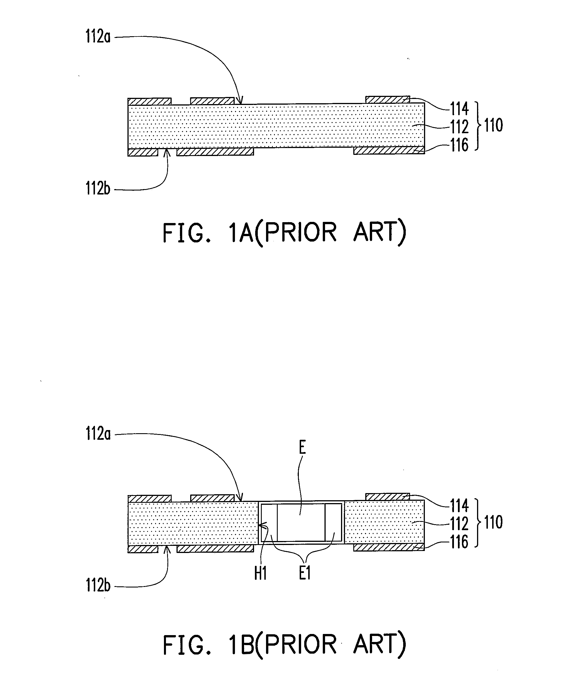
Figure 2 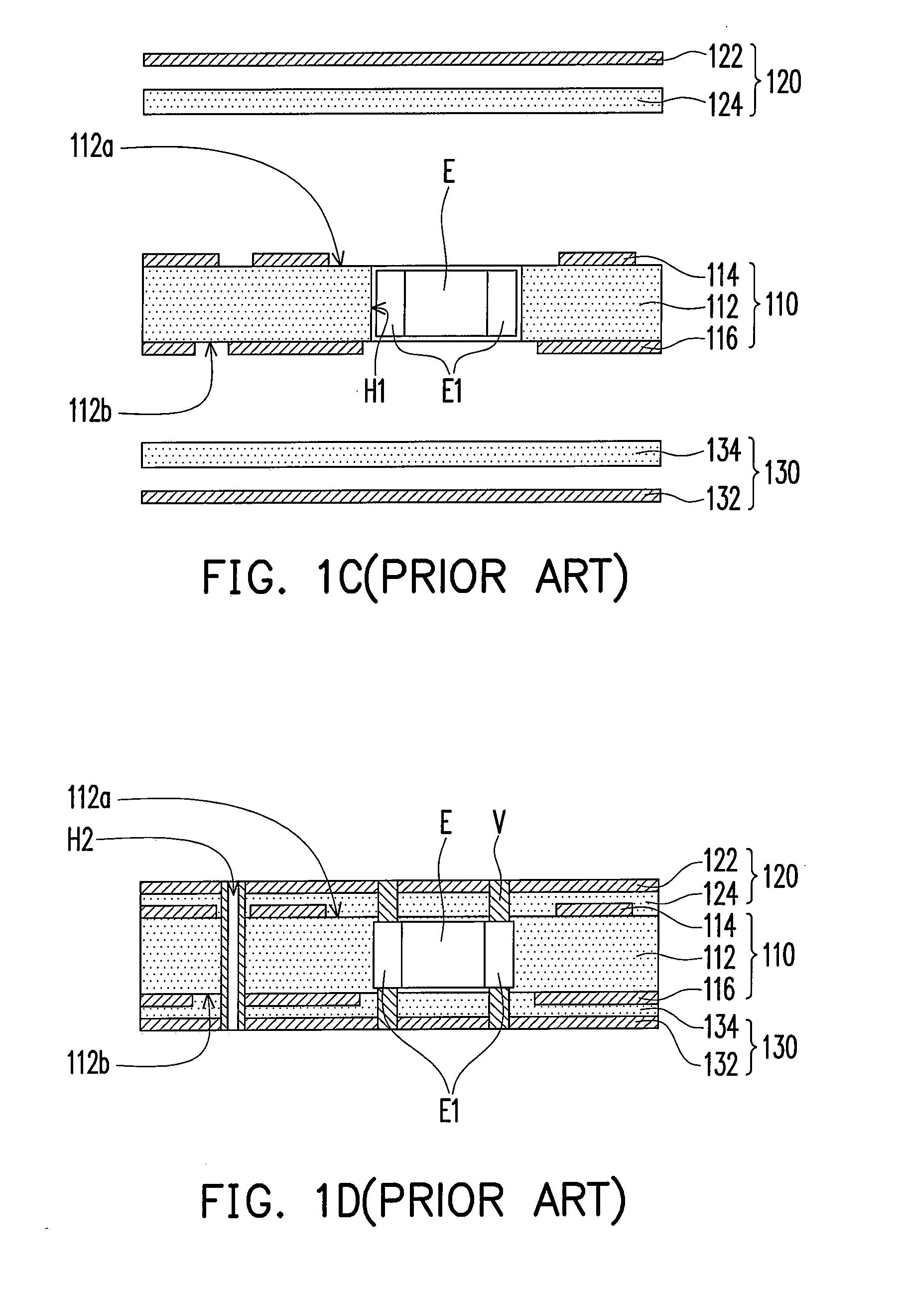
Figure 3
Abstract
Description
CROSS-REFERENCE TO RELATED APPLICATION
[0001] This application claims the priority benefit of Taiwan application serial no. 95104698, filed on Feb. 13, 2006. All disclosure of the Taiwan application is incorporated herein by reference.BACKGROUND OF THE INVENTION
[0002] 1. Field of Invention
[0003] The present invention relates to a method of fabricating a substrate. More particularly, the present invention relates to a method of fabricating a substrate with an embedded component therein.
[0004] 2 . Description of Related Art
[0005] Generally speaking, a circuit substrate is mainly formed through alternately stacking a plurality of patterned circuit layers and dielectric layers, wherein the patterned circuit layers are defined and formed through a lithography and etching process on copper foils, and the dielectric layers are arranged between the patterned circuit layers for isolating two adjacent patterned circuit layers. Additionally, the adjacent patterned circuit layers are electrically con...
Examples
Embodiment Construction
[0036]FIGS. 2A-2J are schematic sectional views of a fabricating flow of a substrate with an embedded component therein according to an embodiment of the present invention. Firstly, referring to FIG. 2A, a core layer 210 including a first dielectric layer 212, a first patterned circuit layer 214, and a second patterned circuit layer 216 is provided. The first patterned circuit layer 214 and the second patterned circuit layer 216 are disposed on an upper surface 212a and a lower surface 212b of the first dielectric layer 212, respectively. In this embodiment, the step of providing the core layer 210 includes patterning a first metal layer (not shown, and the material thereof is copper) and a second metal layer (not shown, and the material thereof is copper) on the upper surface 212a and the lower surface 212b of the first dielectric layer 212 through a lithography and etching process, respectively, so as to form the first patterned circuit layer 214 and the second patterned circuit l...