
Receptacles for inkjet deposited PLED/OLED devices and method of making the same
a technology of inkjet deposited pled/oled devices and pled/oled devices, which is applied in the direction of discharge tube luminescnet screens, discharge tube/lamp details, electric discharge lamps, etc., can solve the problems of complex and costly, high production process costs, and inflexible, and achieve less complex and cost-effective effects
Patent Information
- Authority / Receiving Office
- US · United States
- Patent Type
- Applications(United States)
- Current Assignee / Owner
- Publication Date
- 2007-11-15
- Estimated Expiration
- Not applicable · inactive patent
Smart Images
Figure 1 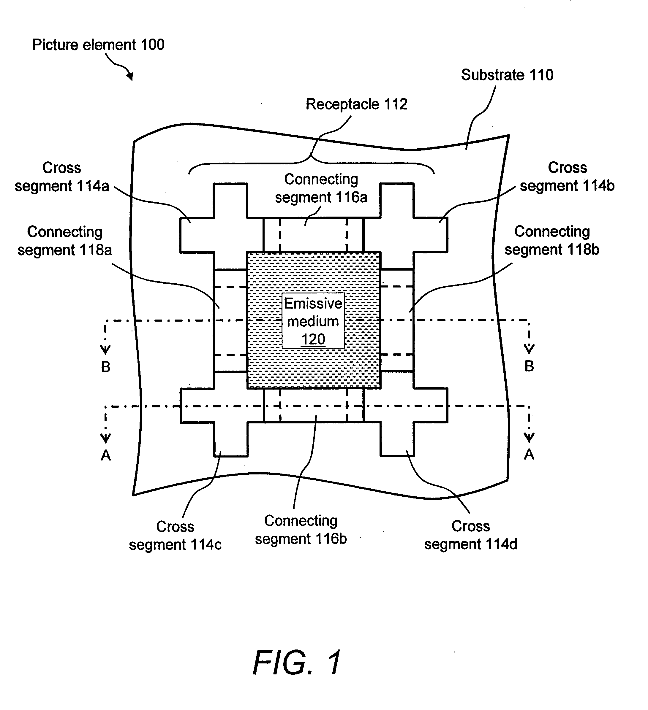
Figure 2 
Figure 3
Abstract
Description
FIELD OF THE INVENTION
[0001] The present invention relates to an inkjet deposition process for forming polymeric light-emitting diode (PLED) or organic light-emitting diode (OLED) displays. In particular, the invention relates to forming evaporated receptacles for inkjet deposited PLED / OLED devices. BACKGROUND OF THE INVENTION
[0002] An organic light-emitting diode (OLED) is a light-emitting diode (LED) made of semiconducting organic polymers. These devices promise to be much cheaper to fabricate than inorganic LEDs. Varying amounts of OLEDs can be deposited in arrays on a screen by use of simple “printing” methods to create a graphical color display, for use as television screens, computer displays, portable system screens, and in advertising and information board applications. OLED panels may also be used as lighting devices.
[0003] One of the great benefits of an OLED display over the traditional liquid crystal displays found in computer monitors is that OLED displays do not req...
Examples
first embodiment
[0023]FIG. 1 illustrates a top view of a picture element 100 in accordance with the invention. Picture element 100 is a representative pixel of a flat-panel display, such as a PLED or OLED display. Picture element 100 includes a substrate 110 upon which is formed a receptacle 112. Receptacle 112 is formed by an arrangement of evaporated segments. Receptacle 112 is formed of a plurality of cross segments 114 arranged on a grid that are interconnected via a plurality of connecting segments 116 and connecting segments 118, which form the walls of receptacle 112 for retaining liquid solvent during an inkjet deposition process.
[0024] In this example, receptacle 112 is formed of a cross segment 114a, a cross segment 114b, a cross segment 114c, and a cross segment 114d, arranged on a grid as shown in FIG. 1. Cross segments 114a and 114b are interconnected via a connecting segment 116a to form a first wall of receptacle 112; cross segments 114c and 114d are interconnected via a connecting s...
second embodiment
[0046]FIG. 6 illustrates a top view of a picture element 600 in accordance with the invention. Picture element 600 is a representative pixel of a flat-panel display, such as a PLED or OLED display. Picture element 600 includes substrate 110, upon which is formed a receptacle 612. Receptacle 612 is formed by an arrangement of evaporated segments and is formed of a plurality of cross segments 614, arranged on a grid, that are interconnected via a plurality of connecting segments 616 and connecting segments 618, which form the walls of receptacle 612 for retaining liquid solvent during an inkjet deposition process.
[0047] In this example, receptacle 612 is formed of a cross segment 614a, a cross segment 614b, a cross segment 614c, and a cross segment 614d, arranged on a grid, as shown in FIG. 6. Cross segments 614a and 614b are interconnected via a connecting segment 616a to form a first wall of receptacle 612; cross segments 614c and 614d are interconnected via a connecting segment 616...