
Method of manufacturing p-type nitride semiconductor and semiconductor device fabricated by the method
a technology of nitride semiconductor and semiconductor device, which is applied in the direction of semiconductor lasers, coatings, lasers, etc., can solve the problems of significantly high resistance and inability to achieve p-type electric properties, and achieve low resistance, prevent thermal damage, and high reproducibility
Patent Information
- Authority / Receiving Office
- US · United States
- Patent Type
- Applications(United States)
- Current Assignee / Owner
- Publication Date
- 2009-05-14
Smart Images
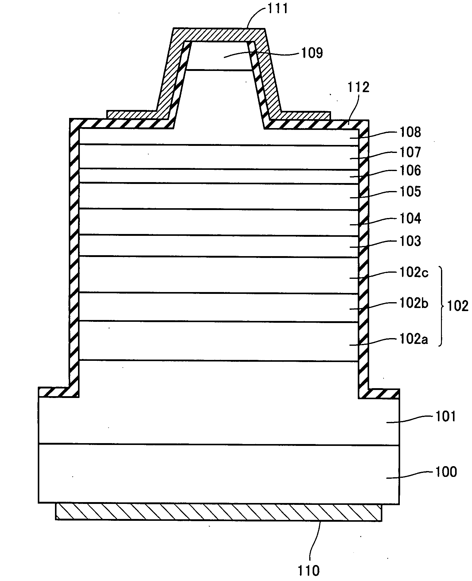
Figure 1 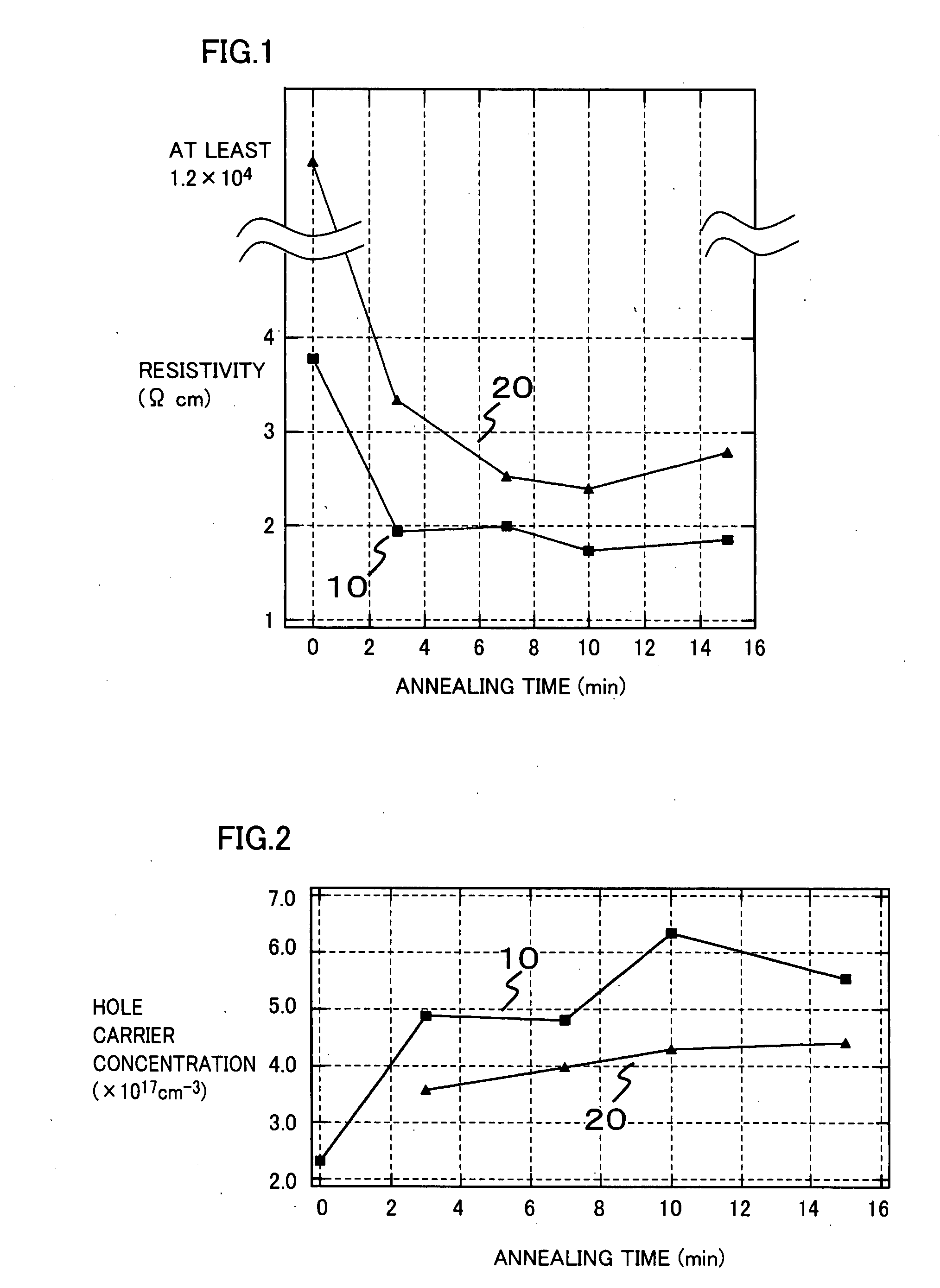
Figure 2 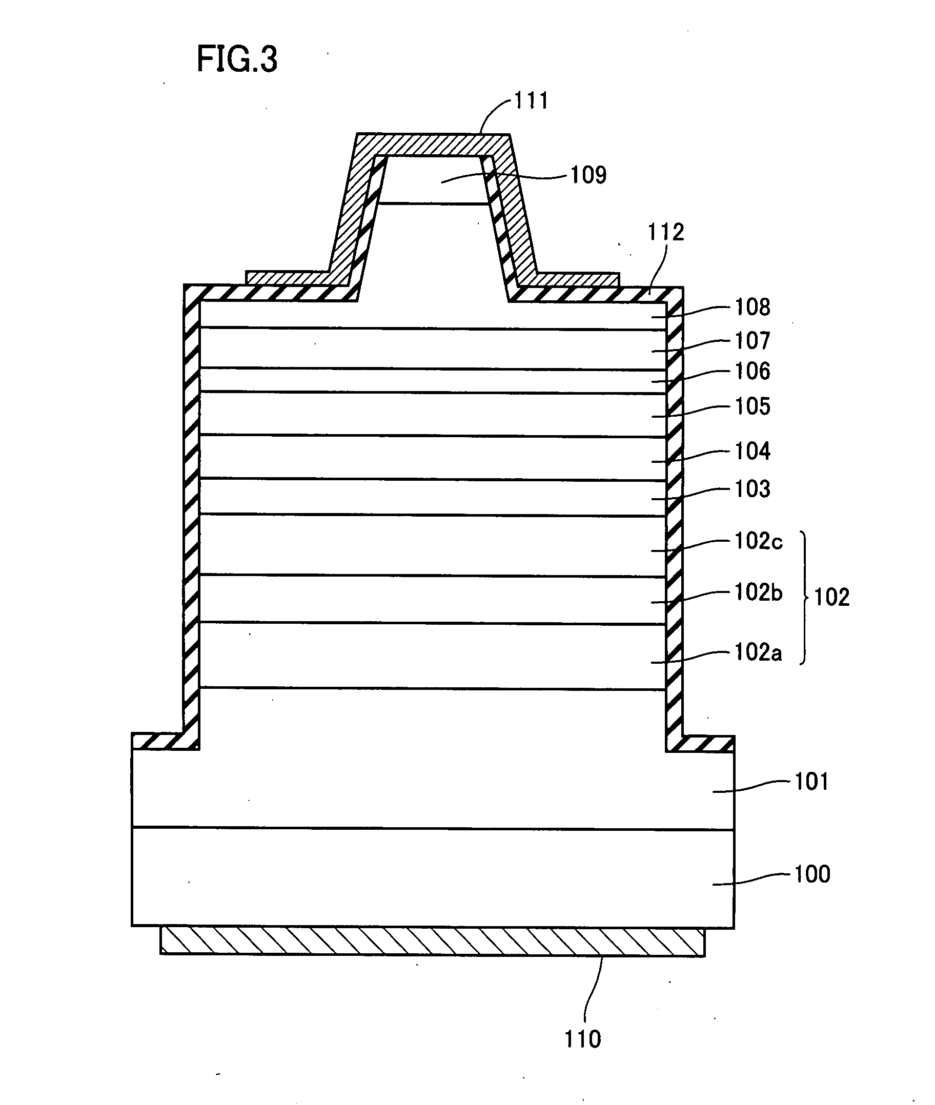
Figure 3
Abstract
Description
TECHNICAL FIELD
[0001] The present invention relates to a method of manufacturing a p-type nitride semiconductor and a semiconductor device fabricated by the method.BACKGROUND ART
[0002] Conventionally, a nitride semiconductor layer fabricated by a metal organic chemical vapor deposition method (MOCVD method) and doped with p-type impurities was electrically neutral and could not obtain a p-type electric property, and had significantly high resistance. Accordingly, Japanese Patent Laying-Open No. 05-183189 (Patent Document 1) describes that, after the completion of crystal growth, the nitride semiconductor layer doped with p-type impurities and having significantly high resistance is subjected to an annealing treatment in an atmosphere that contains substantially no hydrogen and at a temperature of at least 400° C., to thereby eliminate hydrogen from the nitride semiconductor layer, so that a nitride semiconductor having p-type conductivity and low resistance can be obtained from a nitr...
Examples
first embodiment
[0034]A first embodiment can mainly solve the first problem.
[0035]Initially, a substrate is placed in a metal organic chemical vapor deposition device (MOCVD device). Here, the substrate collectively refers to a base material such as sapphire, GaN, AlGaN, SiC, Si, or ZrB2, or the one including a nitride semiconductor layer, a crystal of which is grown on the base material. The substrate is heated to a certain temperature. By using a first carrier gas containing a nitrogen carrier gas and a hydrogen carrier gas of a flow quantity larger than that of the nitrogen carrier gas, a Group III raw material, a raw material containing Mg, and a Group V raw material containing N are supplied to form a nitride semiconductor layer. The step described above is referred to as a first step.
[0036]After the first step, a second step of lowering a temperature of the substrate by using a second carrier gas to which a material containing N is added at a concentration of at least 0.01% and less than 20% ...
second embodiment
[0066]A second embodiment of the present invention can mainly solve the second problem.
[0067]After the first and second steps according to the present invention, the nitride semiconductor layer having a p-type electric property was subjected to an annealing treatment in an inert gas for at least one minute and at most 15 minutes. This is the third step according to the present invention. By adding the third step to the first and second steps according to the present invention, resistivity of the nitride semiconductor layer is further reduced.
[0068]Most important effects obtained in the second embodiment of the present invention (the effects found in Example 2 described below) will be described in advance, and then various modes of the third step will be described, and the effects of the present invention will be described in detail, illustrating specific experimental data in Example 2.
[0069]Clearly, resistivity of a nitride semiconductor layer obtained by subjecting the nitride semi...
example 1
[0077]A detailed example of the first embodiment will hereinafter be described.
[0078]A sample A in the present example was made of a C-plane sapphire substrate (corresponds to the substrate in the present application), an undoped GaN layer of approximately 3 μm provided on the sapphire substrate, and a GaN layer doped with Mg and of approximately 0.6 μm (which corresponds to the nitride semiconductor layer formed in the first step) provided on the undoped GaN layer. A method of manufacturing the Mg-doped GaN layer by the first step of the present invention included the steps of growing the Mg-doped GaN layer by supplying a hydrogen carrier gas and a nitrogen carrier gas at 25 liters per minute and at 6.5 liters per minute, respectively, at a growth temperature of 1030° C., and supplying tri-methyl gallium as a Group III raw material at 40 cc per minute, bis(ethyl cyclopentadienyl) magnesium as a raw material containing Mg at 60 cc per minute, and ammonia as a Group V raw material co...