
Semiconductor chip
a technology of semiconductors and chips, applied in the field of semiconductor chips, can solve the problems of increased ir drop, circuit misoperation, and increase in the possibility of circuit misoperation resulting from increased ir drop, so as to prevent circuit misoperation, reduce the resistance of power supply lines, and increase the chip area
Patent Information
- Authority / Receiving Office
- US · United States
- Patent Type
- Applications(United States)
- Current Assignee / Owner
- Publication Date
- 2009-07-02
Smart Images
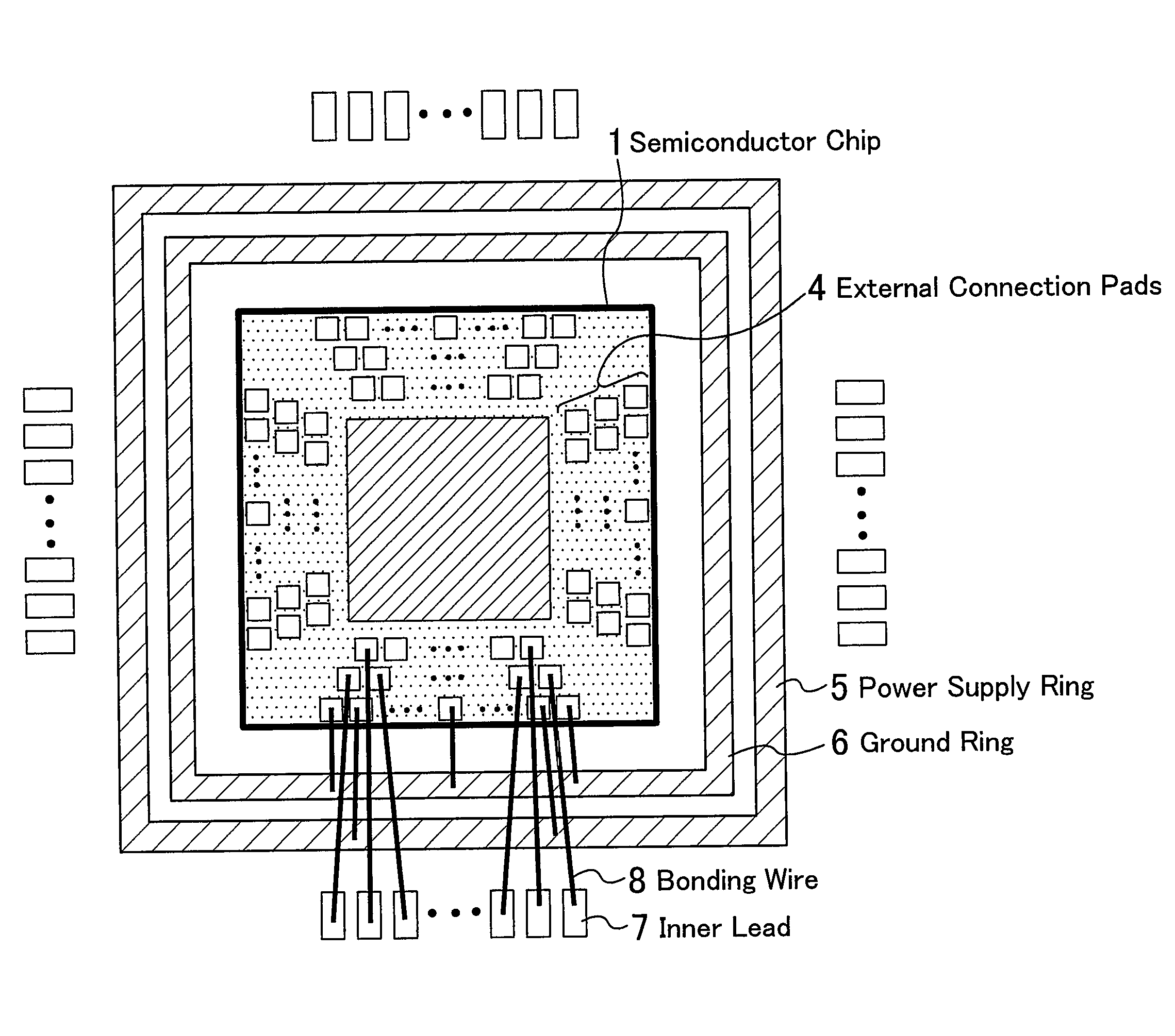
Figure 1 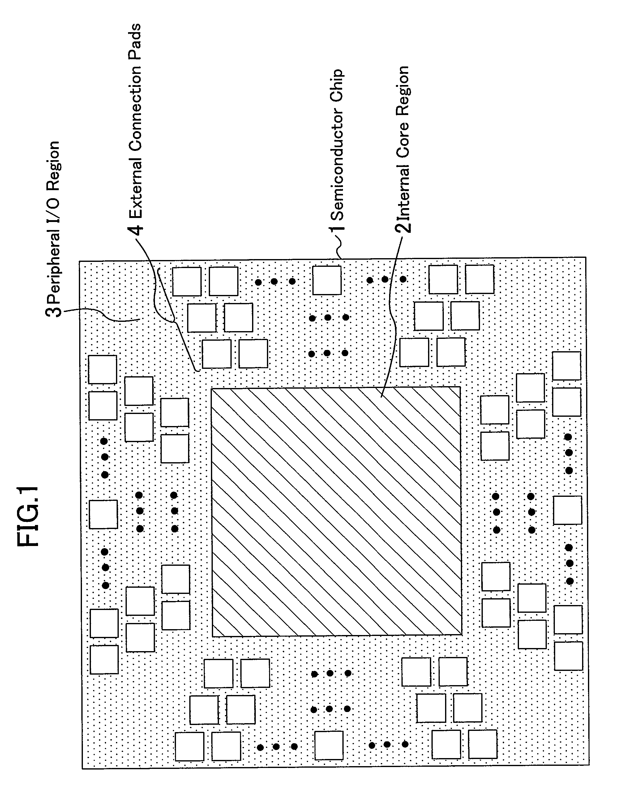
Figure 2 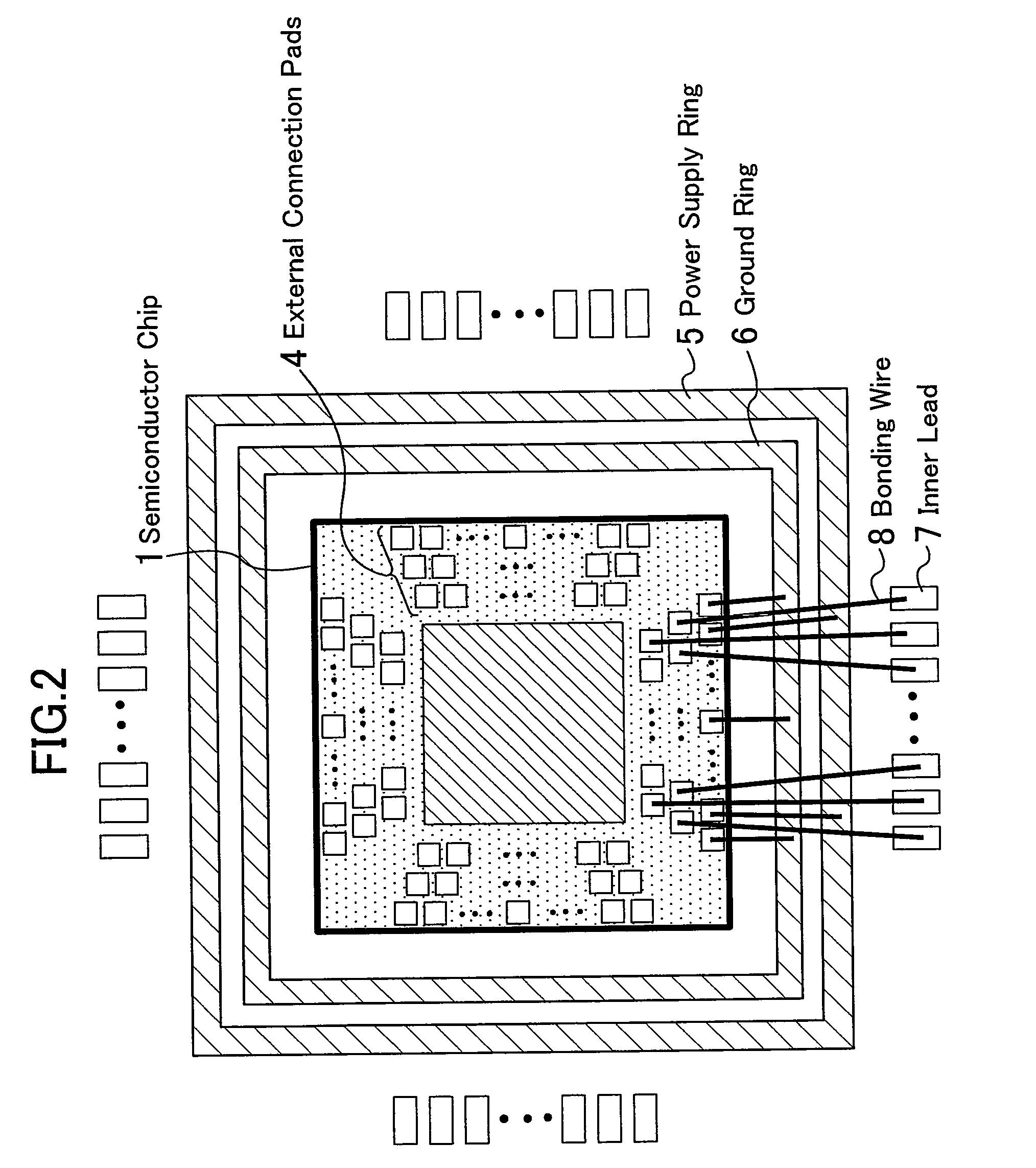
Figure 3
Abstract
Description
CROSS REFERENCE TO RELATED APPLICATION
[0001] This Non-Provisional application claims priority under 35 U.S.C. §119(a) on Patent Application JP 2007-339739, filed Dec. 28, 2007, which are entirely incorporated herein by reference, inclusive of the specification, drawings, and claims.FIELD OF THE INVENTION
[0002] The present invention relates to a semiconductor chip in which external connection pads are arranged at a peripheral portion thereof.DESCRIPTION OF THE RELATED ART
[0003] As a conventional semiconductor chip, a structure has been adopted in which an internal core region formed with an internal core circuit is provided at the center portion thereof, a peripheral I / O region formed with an interface circuit is provided outside the internal core region, and external connection pads are arranged in a staggered configuration at the peripheral portion thereof.
[0004] Patent Document 1 discloses a structure as a semiconductor chip having external connection pads arranged in two rows in a st...
Examples
embodiment 1
[0041]FIG. 1 is a schematic view of a structure of a semiconductor chip which is assumed in each of the first to fourth embodiments of the present invention. The semiconductor chip 1 shown in FIG. 1 includes an internal core region 2 provided at the center portion thereof, and formed with an internal core circuit, and a peripheral I / O region 3 provided outside the internal core region 2, and formed with an interface circuit (I / O circuit). At the peripheral portion of the semiconductor chip 1, a plurality of external connection pads 4 are arranged in three rows in a staggered configuration. To the external connection pads 4, I / O cells in the interface circuit are connected individually.
[0042]FIG. 2 is a view showing a state where the semiconductor chip 1 of FIG. 1 is mounted on a BGA (Ball Grid Array) package. In the BGA package, a dedicated plane for a power supply voltage and a ground voltage is provided, and a common power supply ring 5 and a common ground ring 6 are disposed on t...
embodiment 2
[0050]FIG. 4 is a plan view partly showing a configuration of the external connection pads in the semiconductor chip according to the second embodiment of the present invention. In FIG. 4 also, the external connection pads 4 are arranged in three rows in a staggered configuration, and the I / O cells 9 are arranged correspondingly to the individual external connection pads 4 in the same manner as in FIG. 3A.
[0051]In the present embodiment, of the plurality of external connection pads 4, the first external connection pad 11 which is arranged in the outermost row is used as the power supply pad or the ground pad for the internal core circuit, as shown in FIG. 4. The first external connection pad 11 is connected to the second external connection pad 12 which is arranged in the second outermost row and adjacent to the first external connection pad 11 with the metal 15 in the same layer as the pad metal. In this point, the second embodiment is the same as the first embodiment.
[0052]Further...
embodiment 3
[0055]FIG. 5 is a plan view partly showing a configuration of the external connection pads in the semiconductor chip according to the third embodiment of the present invention. In FIG. 5 also, the external connection pads 4 are arranged in three rows in a staggered configuration, and the I / O cells 9 are arranged correspondingly to the individual external connection pads 4 in the same manner as in FIG. 3A.
[0056]In the present embodiment, of the plurality of external connection pads 4, the first external connection pad 11 which is arranged in the outermost row is used as the power supply pad or the ground pad for the internal core circuit, as shown in FIG. 5. The first external connection pad 11 is connected to the second external connection pad 12 which is arranged in the second outermost row and adjacent to the first external connection pad 11 with the metal 15 in the same layer as the pad metal. In this point, the third embodiment is the same as the first embodiment.
[0057]Further, ...