
Thin film transistor array panel and manufacturing method of the same
a technology of thin film transistors and array panels, which is applied in the direction of transistors, optics, instruments, etc., can solve the problems of alignment errors, inability to align pixel electrodes, and difficulty in manufacturing liquid crystal displays, so as to increase the aperture ratio and minimize the overall area of the partition
Patent Information
- Authority / Receiving Office
- US · United States
- Patent Type
- Applications(United States)
- Current Assignee / Owner
- Publication Date
- 2010-01-07
Smart Images
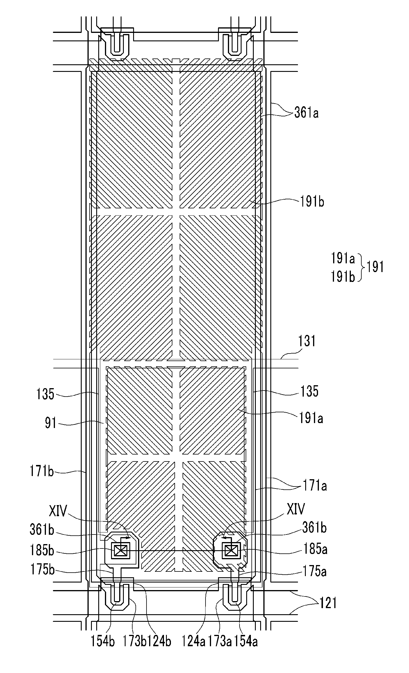
Figure 1 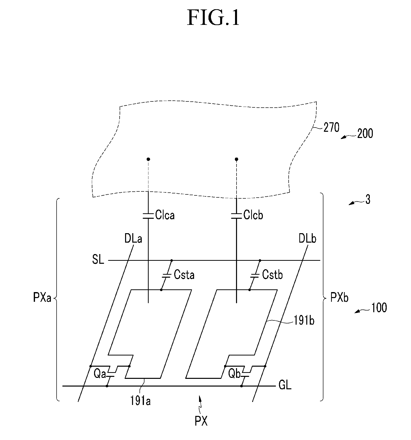
Figure 2 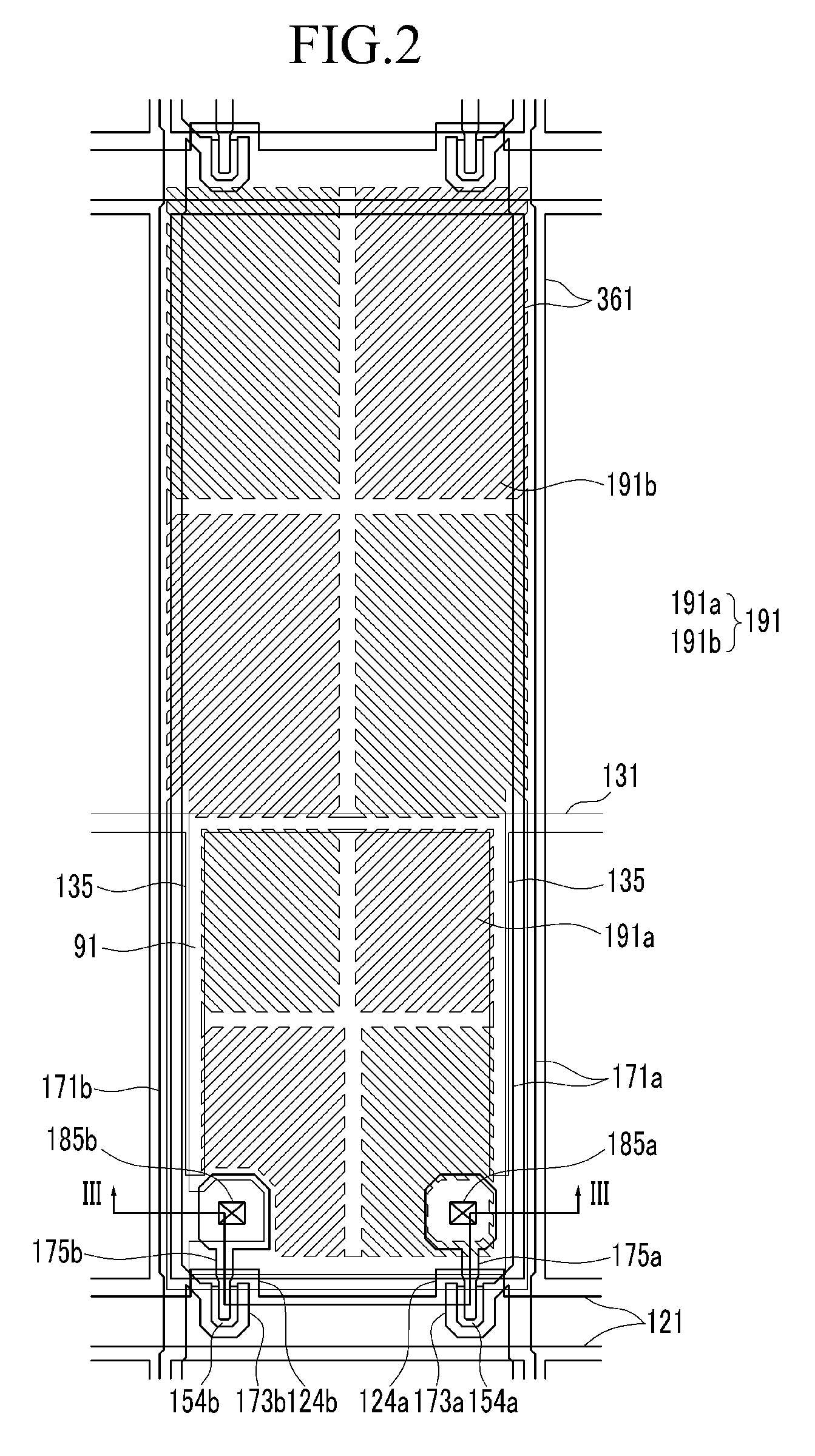
Figure 3
Abstract
Description
[0001] This application claims priority to Korean Patent Application No. 10-2008-0065548 filed on Jul. 7, 2008, and all the benefits accruing therefrom under 35 U.S.C. §119, the entire contents of which are incorporated herein by reference.BACKGROUND OF THE INVENTION
[0002] (a) Field of the Invention
[0003] The present invention relates to a thin film transistor array panel and a manufacturing method thereof.
[0004] (b) Description of the Related Art
[0005] A liquid crystal display (“LCD”) is one of the most widely used flat panel displays (“FPD”), and it is composed of two display panels on which field generating electrodes are formed, and a liquid crystal layer interposed between the two display panels. A voltage is applied to the field generating electrodes to generate an electric field on the liquid crystal layer, and the orientation of liquid crystal molecules of the liquid crystal layer is determined and the polarization of incident light is controlled through the generated electric fi...
Examples
Embodiment Construction
[0033]The present invention will be described more fully hereinafter with reference to the accompanying drawings, in which exemplary embodiments of the invention are shown. As those skilled in the art would realize, the described embodiments may be modified in various different ways, all without departing from the spirit or scope of the present invention.
[0034]In the drawings, the thickness of layers, films, panels, regions, etc., are exaggerated for clarity. Like reference numerals designate like elements throughout the specification. It will be understood that when an element such as a layer, film, region, or substrate is referred to as being “on” another element, it can be directly on the other element or intervening elements may also be present. In contrast, when an element is referred to as being “directly on” another element, there are no intervening elements present.
[0035]It will be understood that, although the terms first, second, third, etc., may be used herein to describe...