
Method of making a semiconductor chip assembly with a post/base heat spreader and horizontal signal routing
a technology of semiconductor chip and post/base heat spreader, which is applied in the manufacture of printed circuits, printed circuit aspects, basic electric elements, etc., can solve the problems of heat not only degrading the chip, short life span and immediate failure of the semiconductor device at high operating temperature, and easy degradation of performance, etc., to achieve excellent heat spreading and heat dissipation, low cost, and low thermal conductivity
Patent Information
- Authority / Receiving Office
- US · United States
- Patent Type
- Applications(United States)
- Current Assignee / Owner
- Publication Date
- 2010-01-07
- Estimated Expiration
- Not applicable · inactive patent
Smart Images
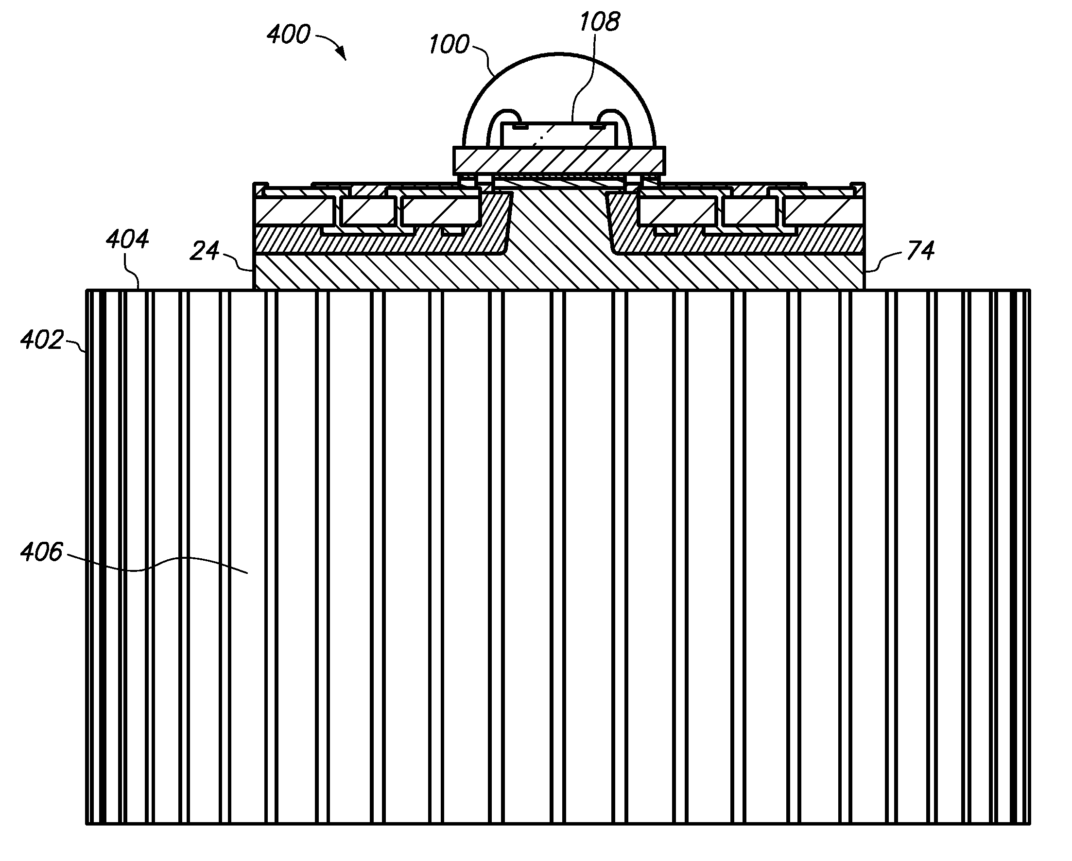
Figure 1 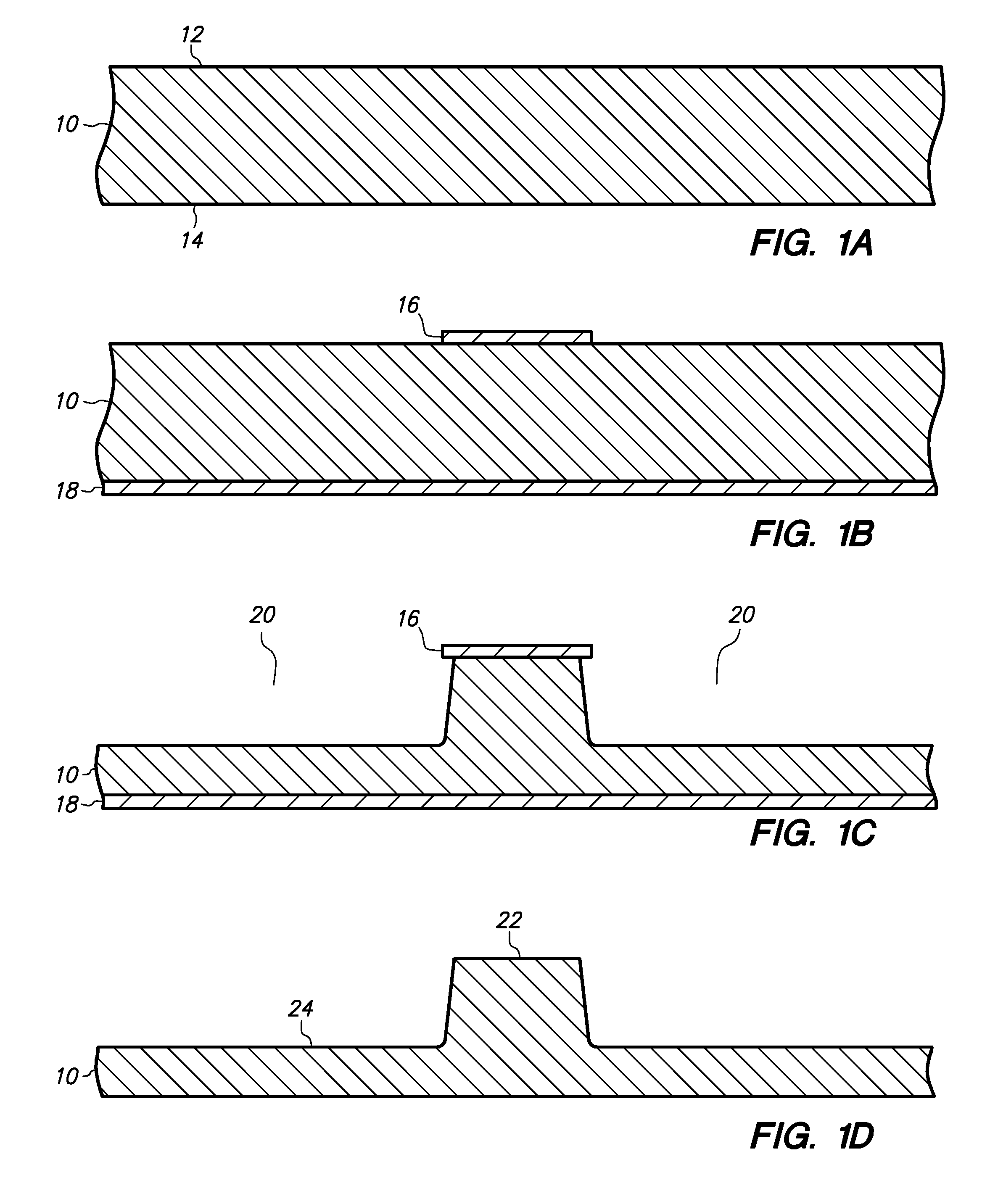
Figure 2 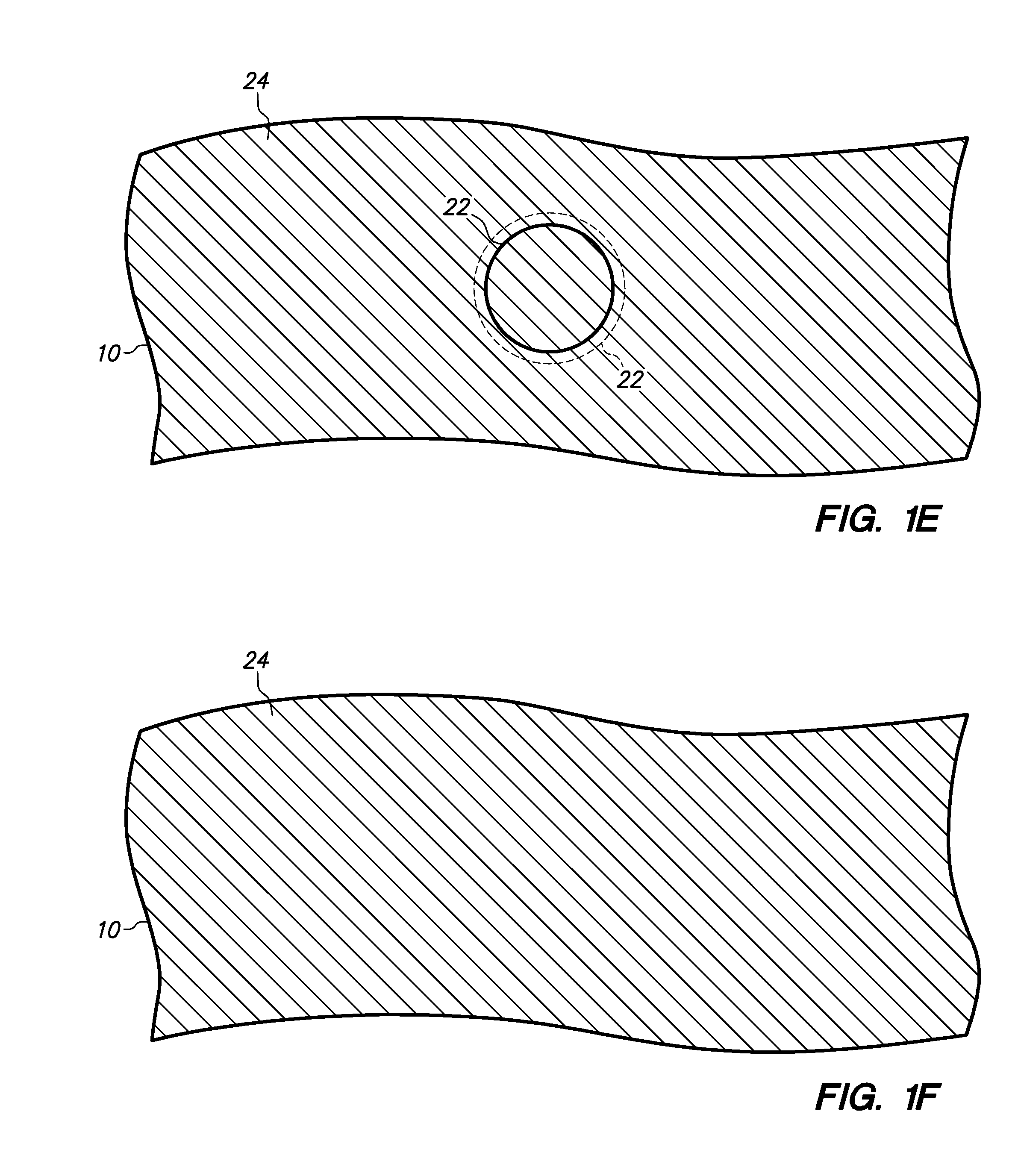
Figure 3
Abstract
Description
CROSS-REFERENCE TO RELATED APPLICATIONS
[0001] This application is a continuation-in-part of U.S. application Ser. No. 12 / 406,510 filed Mar. 18, 2009, which claims the benefit of U.S. Provisional Application Ser. No. 61 / 071,589 filed May 7, 2008, U.S. Provisional Application Ser. No. 61 / 071,588 filed May 7, 2008, U.S. Provisional Application Ser. No. 61 / 071,072 filed Apr. 11, 2008, and U.S. Provisional Application Ser. No. 61 / 064,748 filed Mar. 25, 2008, each of which is incorporated by reference.
[0002] This application also claims the benefit of U.S. Provisional Application Ser. No. 61 / 150,980 filed Feb. 9, 2009, which is incorporated by reference.BACKGROUND OF THE INVENTION
[0003] 1. Field of the Invention
[0004] The present invention relates to semiconductor chip assembly, and more particularly to a semiconductor chip assembly with a semiconductor device, a substrate, an adhesive and a heat spreader and its method of manufacture.
[0005] 2. Description of the Related Art
[0006] Semiconductor...
Examples
Embodiment Construction
[0074]FIGS. 1A-1D are cross-sectional views showing a method of making a post and a base in accordance with an embodiment of the present invention, and FIGS. 1E and 1F are top and bottom views, respectively, corresponding to FIG. 1D.
[0075]FIG. 1A. is a cross-sectional view of metal plate 10 which includes opposing major surfaces 12 and 14. Metal plate 10 is illustrated as a copper plate with a thickness of 500 microns. Copper has high thermal conductivity, good bondability and low cost. Metal plate 10 can be various metals such as copper, aluminum, alloy 42, iron, nickel, silver, gold, combinations thereof, and alloys thereof.
[0076]FIG. 1B is a cross-sectional view of etch mask 16 and cover mask 18 formed on metal plate 10. Etch mask 16 and cover mask 18 are illustrated as photoresist layers which are deposited on metal plate 10 using dry film lamination in which hot rolls simultaneously press photoresist layers 16 and 18 onto surfaces 12 and 14, respectively. Wet spin coating and c...