
Progressive trimming method
Patent Information
- Authority / Receiving Office
- US · United States
- Current Assignee / Owner
- Publication Date
- 2011-04-28
Smart Images
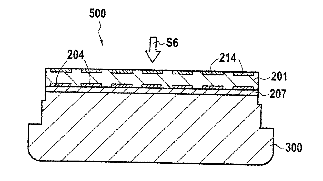
Figure 1 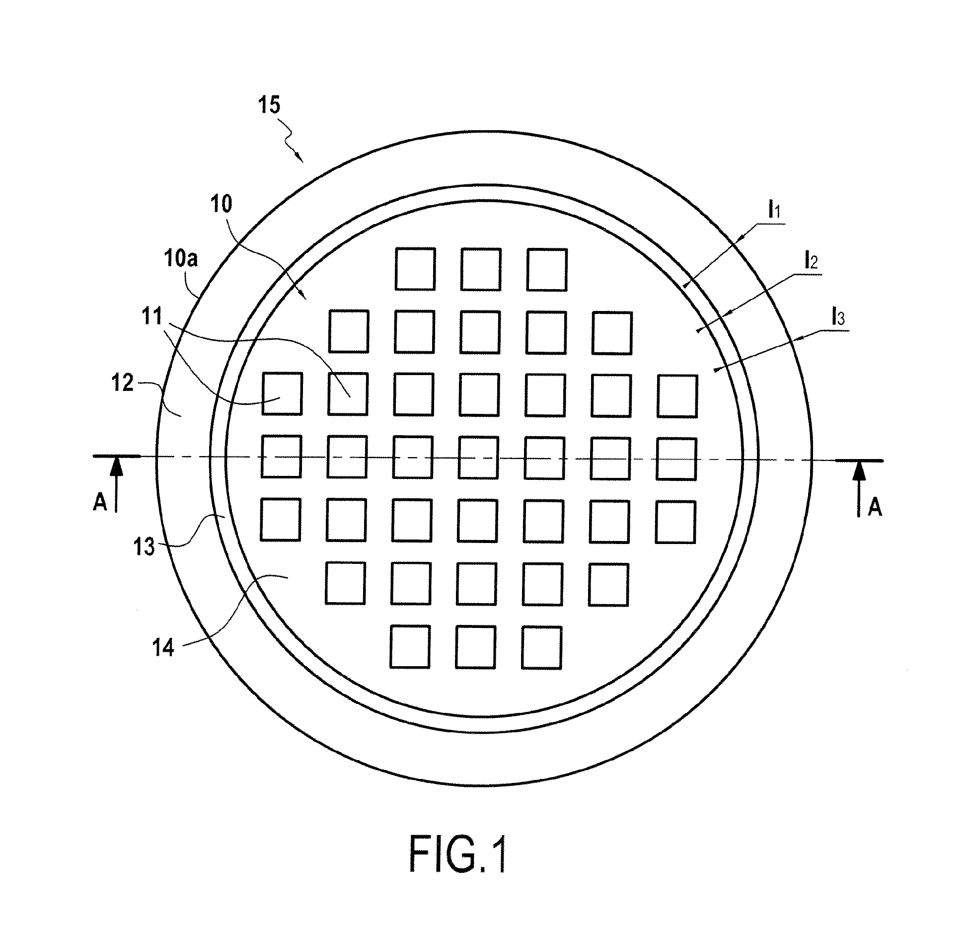
Figure 2 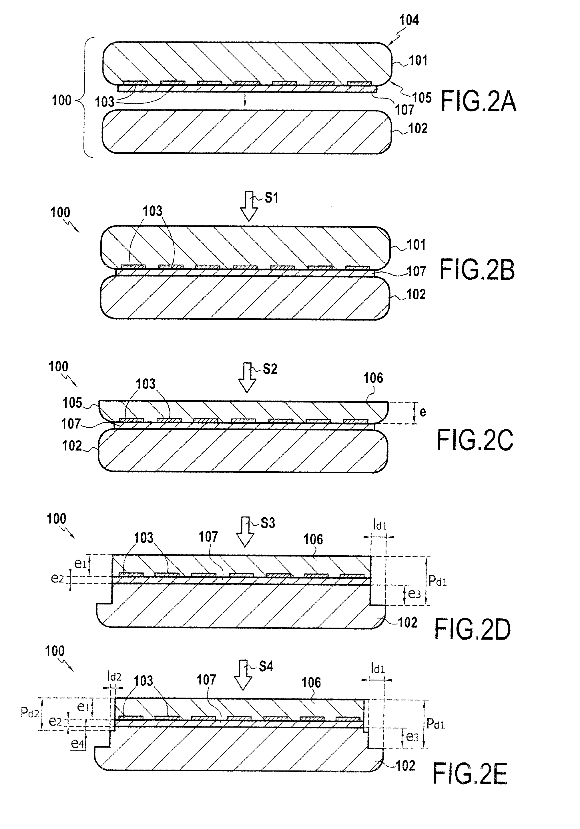
Figure 3
Abstract
Description
FIELD OF THE INVENTION AND PRIOR ART
[0001] The present invention relates to the field of producing multilayer semiconductor structures or substrates (also termed multilayer semiconductor wafers) produced by transfer of at least one layer onto a support. The transferred layer is formed by molecular bonding of a first wafer onto a second wafer or support, the first wafer generally being thinned following bonding. The first wafer may also include all or part of a component or a plurality of microcomponents, as happens with three-dimensional (3D) integration of components, which requires transfer of one or more layers of microcomponents onto a final support, and also as happens with circuit transfer as, for example, in the fabrication of back lit imaging devices.
[0002] The edges of the wafers used to form the transferred layers and the supports generally have chamfers or edge roundings serving to facilitate their manipulation and to avoid breakages at the edges that could occur if those e...
Examples
Embodiment Construction
[0026]The present invention is of general application to trimming a structure comprising at least two wafers assembled together by molecular bonding or any other type of bonding such as anodic bonding, metallic bonding, or bonding with adhesive, it being possible for components to be formed beforehand in the first wafer that is then bonded to the second wafer that constitutes a support. The wafers are generally of circular outline, possibly with different diameters, in particular diameters of 100 millimeters (mm), 200 mm, or 300 mm. The term “components” as used here means any type of element produced with materials that differ from the material of the wafer and that are sensitive to the high temperatures normally used to reinforce the bonding interface. These components correspond in particular to elements forming all or a portion of an electronic component or a plurality of electronic microcomponents, such as circuits or contacts or active layers that may be damaged or even destro...