
Method for driving plasma display panel and plasma display device
a plasma display panel and plasma display technology, applied in the direction of instruments, computing, electric digital data processing, etc., can solve the problems of non-uniform display luminance and damage to image display quality, and achieve the effect of preventing luminance reduction of display image, reducing afterimage phenomenon, and reducing the strength level of afterimag
Patent Information
- Authority / Receiving Office
- US · United States
- Patent Type
- Applications(United States)
- Current Assignee / Owner
- Publication Date
- 2012-07-05
- Estimated Expiration
- Not applicable · inactive patent
Smart Images
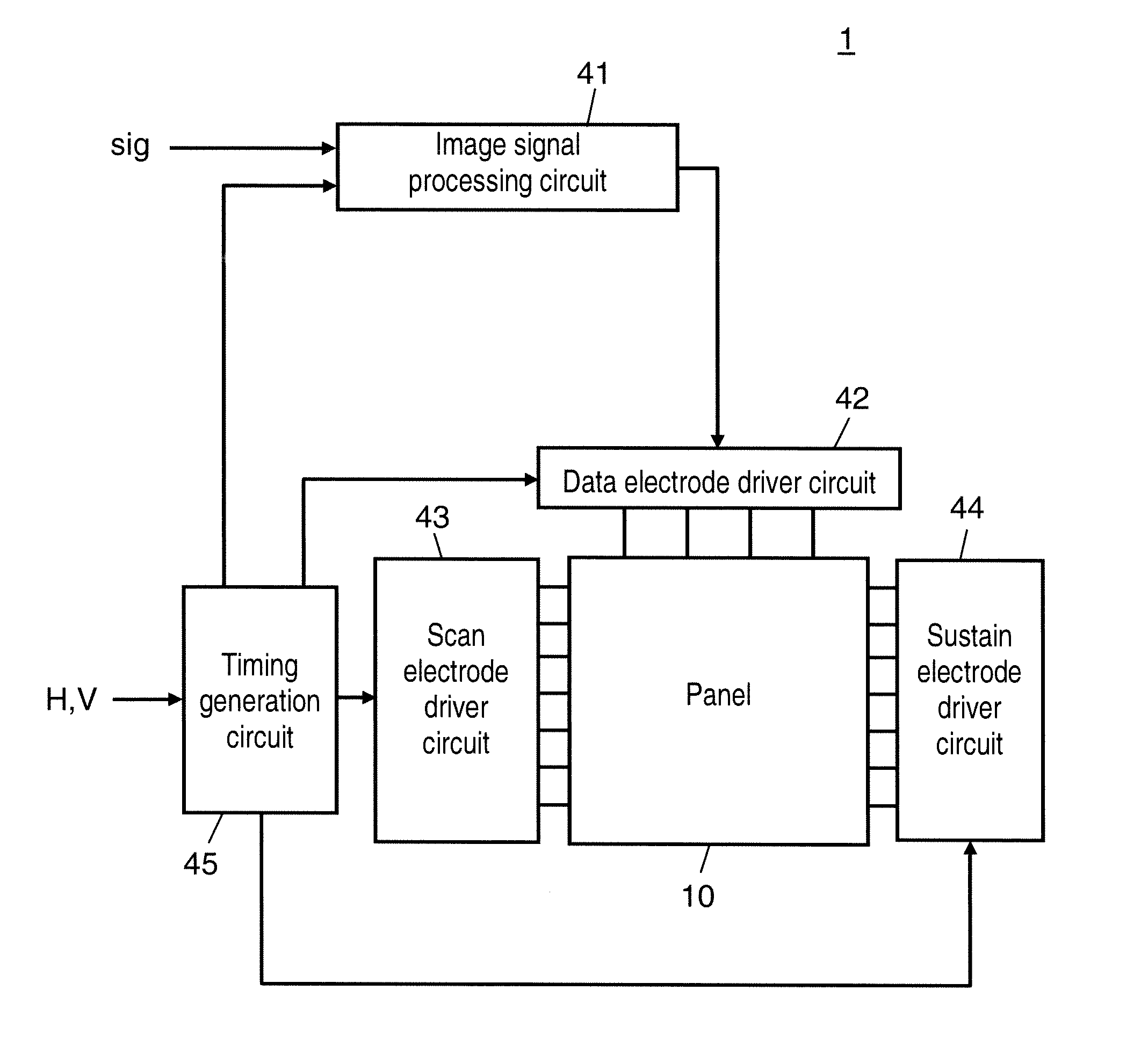
Figure 1 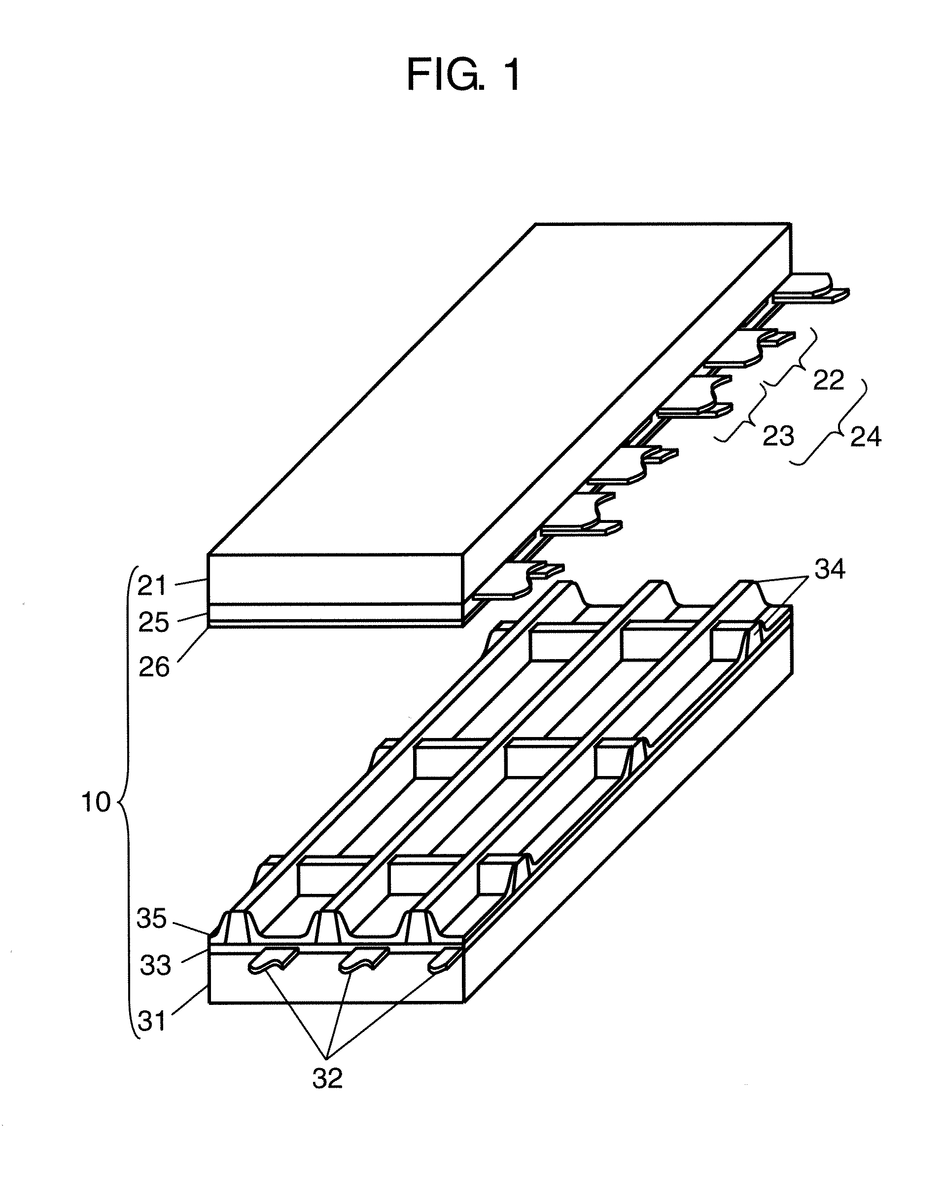
Figure 2 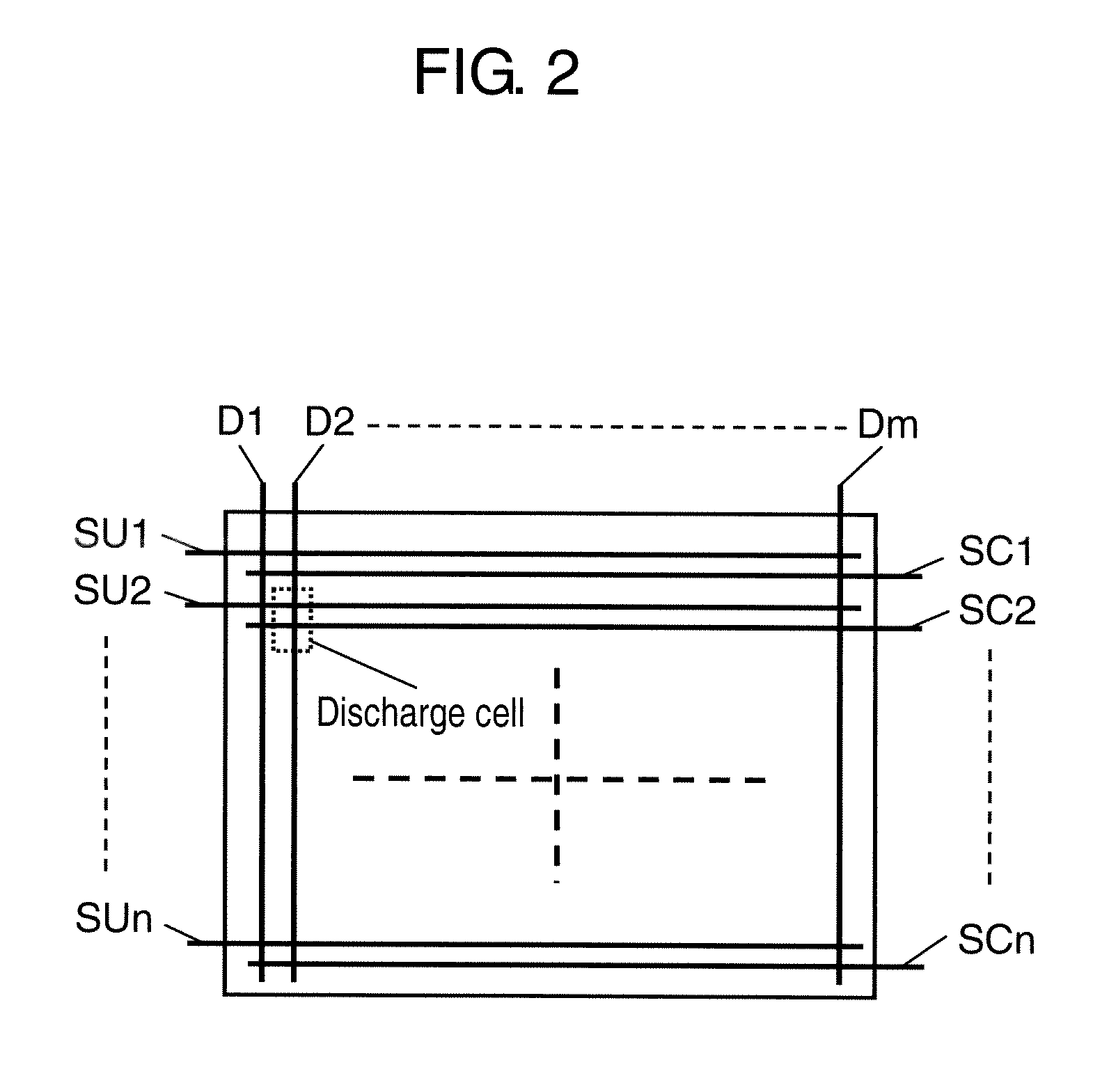
Figure 3
Abstract
Description
TECHNICAL FIELD
[0001] The present application relates to a driving method of a plasma display panel and a plasma display apparatus that are used in a television or a large monitor.BACKGROUND ART
[0002] An alternating-current surface discharge type panel such as a plasma display panel (hereinafter referred to as “panel”) has many discharge cells between a front plate and a rear plate that are faced to each other. The front plate has the following elements:
[0003] a plurality of display electrode pairs disposed in parallel on a front glass substrate; and
[0004] a dielectric layer and a protective layer for covering the display electrode pairs.Here, each display electrode pair is formed of a pair of scan electrode and sustain electrode. The rear plate has the following elements:
[0005] a plurality of data electrodes disposed in parallel on a rear glass substrate;
[0006] a dielectric layer for covering the data electrodes;
[0007] a plurality of barrier ribs disposed on the dielectric layer in parall...
Examples
first exemplary embodiment
[0092]FIG. 1 is an exploded perspective view showing the structure of panel 10 used in a plasma display apparatus in accordance with a first exemplary embodiment of the present invention. A plurality of display electrode pairs 24 formed of scan electrodes 22 and sustain electrodes 23 is disposed on glass-made front plate 21. Dielectric layer 25 is formed so as to cover scan electrodes 22 and sustain electrodes 23, and protective layer 26 is formed on dielectric layer 25. Protective layer 26 is made of a material mainly made of magnesium oxide (MgO).
[0093]A plurality of data electrodes 32 is formed on rear plate 31, dielectric layer 33 is formed so as to cover data electrodes 32, and mesh barrier ribs 34 are formed on dielectric layer 33. Phosphor layers 35 for emitting lights of respective colors of red (R), green (G), and blue (B) are formed on the side surfaces of barrier ribs 34 and on dielectric layer 33.
[0094]Front plate 21 and rear plate 31 face to each other so that display e...
second exemplary embodiment
[0206]In the first exemplary embodiment, the configuration has been described where the luminance gradation value is changed in response to the afterimage strength level of each pixel. However, the following configuration may be employed: when an afterimage phenomenon occurs, the luminance gradation value is changed in response to the afterimage strength level only in a pixel where the luminance gradation value is high (the pixel having a luminance gradation value equal to a predetermined high luminance threshold or higher) and the conspicuous afterimage phenomenon occurs.
[0207]FIG. 10 is a circuit block diagram showing one configuration example of correcting circuit 83 in accordance with a second exemplary embodiment of the present invention. In the second exemplary embodiment, the procedure until the afterimage strength level of each pixel is calculated is similar to that of the first exemplary embodiment, so that only correcting circuit 83 having a configuration different from th...
third exemplary embodiment
[0216]In an image where average picture level (hereinafter referred to as “APL”) during display is high, the luminance is high in whole, hence variation in luminance between adjacent pixels is small, and the number of edges is also small. In other words, in an image of high APL, an afterimage phenomenon is considered to hardly occur comparing with an image of low APL. Therefore, the following configuration may be employed: the APL of an image signal is detected, and the afterimage strength level is changed in response to the APL so that the afterimage strength level is lower when the APL is high than when the APL is low.
[0217]FIG. 11 is a circuit block diagram showing one configuration example of correcting circuit 84 in accordance with a third exemplary embodiment of the present invention. In the third exemplary embodiment, the procedure until the afterimage strength level of each pixel is calculated is similar to that of the first exemplary embodiment, so that only correcting circ...