
Donor substrate, patterning method, and method for producing device
a technology of patterning method and substrate, applied in the direction of sustainable manufacturing/processing, instruments, final product manufacturing, etc., can solve the problems of uneven film thickness, difficult to stably realize fine patterning at low cost, and not a technique in which high-accuracy patterning is realized. achieve the effect of low cos
Patent Information
- Authority / Receiving Office
- US · United States
- Current Assignee / Owner
- Publication Date
- 2012-09-13
- Estimated Expiration
- Not applicable · inactive patent
Smart Images
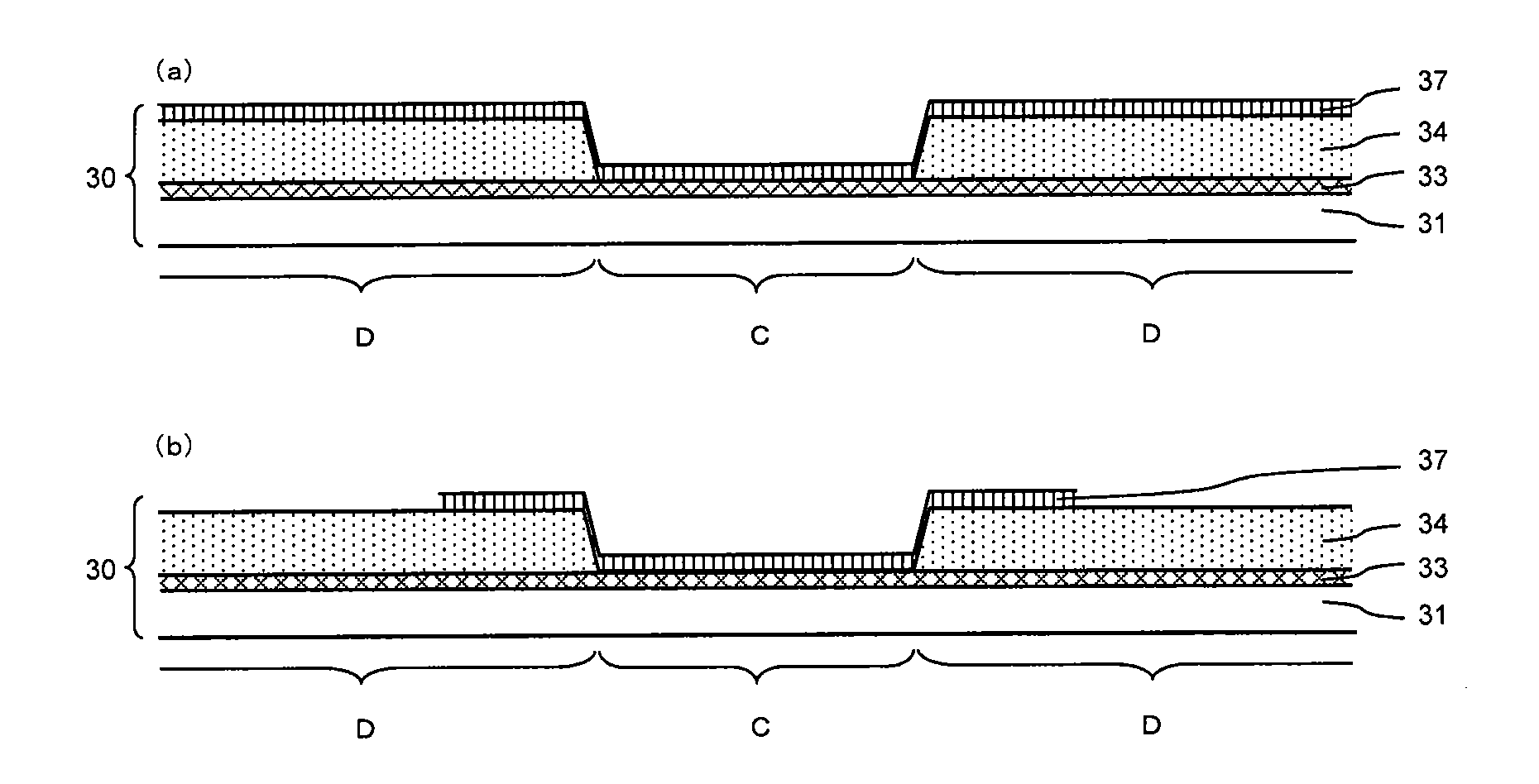
Figure 1 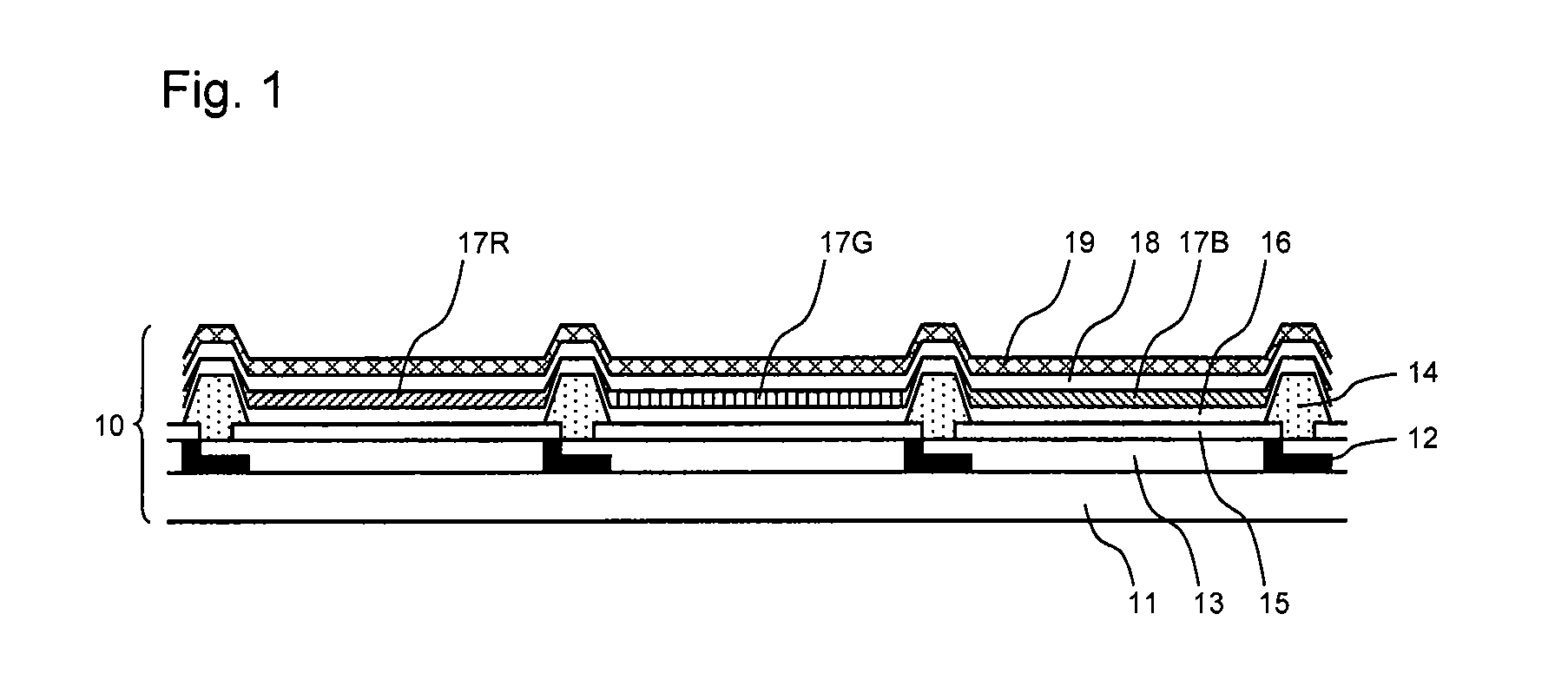
Figure 2 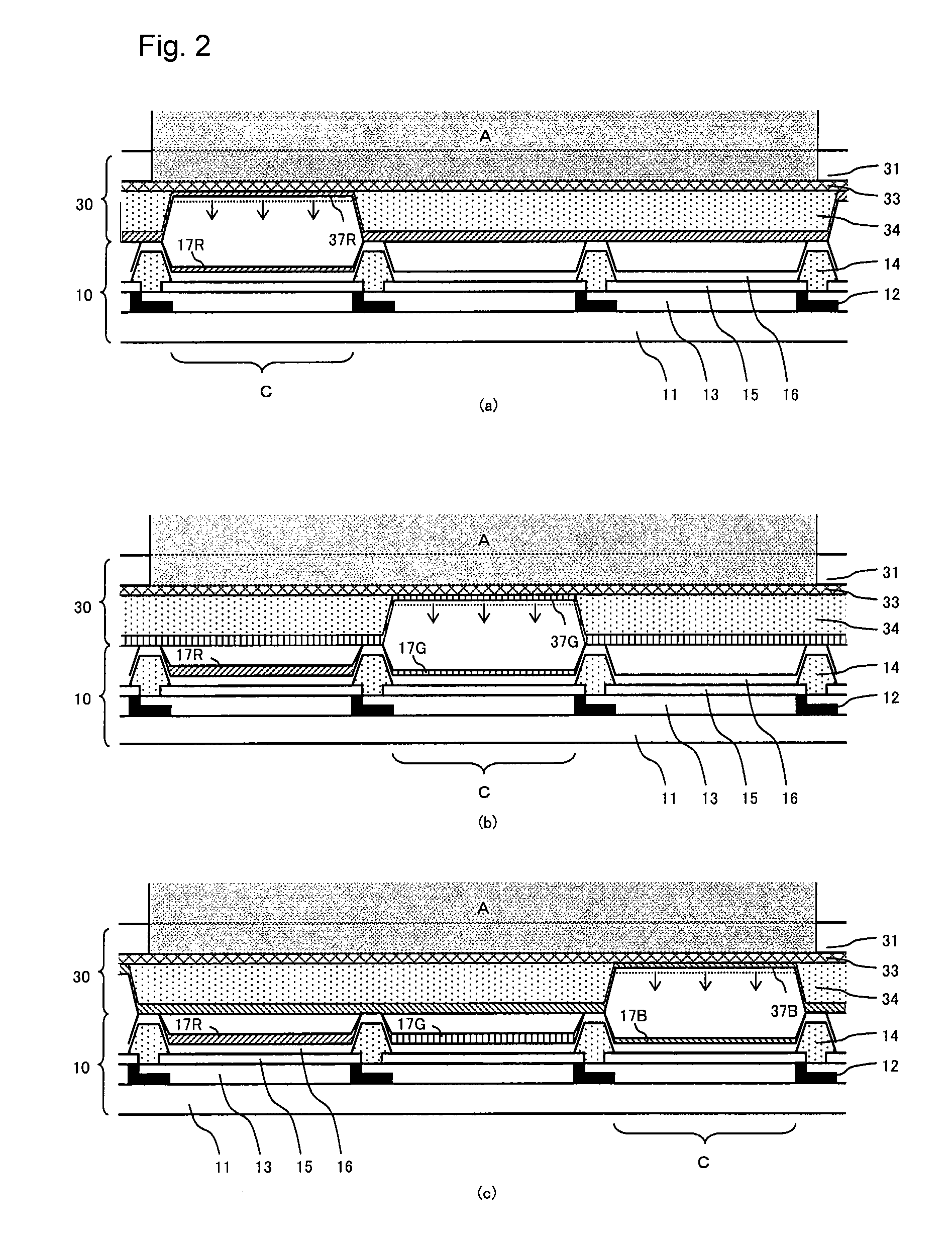
Figure 3
Abstract
Description
CROSS REFERENCE TO RELATED APPLICATIONS
[0001] This application is the U.S. National Phase application of PCT International Application No. PCT / JP2010 / 071431, filed Dec. 1, 2010, and claims priority to Japanese Patent Application No. 2009-275266, filed Dec. 3, 2009, the disclosure of both are incorporated herein by reference in their entireties for all purposes.FIELD OF THE INVENTION
[0002] The present invention relates to a method for patterning a thin film which constitutes devices such as organic light emitting devices, organic TFTs, photoelectric transducers and various sensors, and a method for producing a device using such a patterning method.BACKGROUND OF THE INVENTION
[0003] An organic light emitting device is a light emitting device in which electrons injected from a cathode and holes injected from an anode are recombined in an organic emitting layer interposed between both electrodes. Since C. W. Tang et al. of Eastman Kodak Company have showed that an organic light emitting dev...
Examples
example 1
[0126]A donor substrate was prepared as follows. An alkali-free glass substrate was used as a support. After cleaning and a UV-ozone treatment of the substrate, a tantalum film having a thickness of 0.4 μm was formed on the whole surface as a light-to-heat conversion layer by the sputtering method on the whole surface. Subsequently, the light-to-heat conversion layer was subjected to a UV-ozone treatment. On this layer, a positive-type polyimide photosensitive coating agent (DL-1000, manufactured by TORAY INDUSTRIES, INC.) was spin-coated. The obtained coating film was subjected to prebaking and exposure by UV light so as to obtain a pattern of the objective transfer prevention layer, and then the exposed portion was dissolved and removed by a developing solution (ELM-D, manufactured by TORAY INDUSTRIES, INC.). The thus patterned polyimide precursor film was baked by a hot plate at 320° C. for 10 minutes to form a transfer prevention layer of polyimide. The thickness of the transfer...
example 2
[0132]In the same manner as in Example 1, except that a 0.2 μm thick tantalum film was formed on the whole surface as the first light-to-heat conversion layer in the production of the donor substrate, an operation was carried out up to patterning of the transfer prevention layer. Then, a 0.2 μm thick tantalum film was formed on the whole surface as a second light-to-heat conversion layer. Namely, the donor substrate of the present Example has a structure that a 0.4 μm thick tantalum film is formed in a transfer region, and a polyimide-based transfer prevention layer is sandwiched between two tantalum films in an antitransfer region. In the same manner as in Example 1, a 40 nm thick transferring material layer was formed on almost the whole surface of the substrate.
[0133]In the same manner as in Example 1, except for others, an organic light emitting device was produced. As a result, almost the same emission efficiency as that in Example 1 was obtained. Furthermore, in the donor subs...