
Solar cell panel
a solar cell and panel technology, applied in the field of solar cell panels, can solve the problems of increasing the cost of installing the insulating barrier, the weight of prior art solar cell panels, and the increase in the cost of solar cell panels. achieve the effect of adequate safety margin
Patent Information
- Authority / Receiving Office
- US · United States
- Patent Type
- Applications(United States)
- Current Assignee / Owner
- Publication Date
- 2017-08-03
- Estimated Expiration
- Not applicable · inactive patent
Smart Images
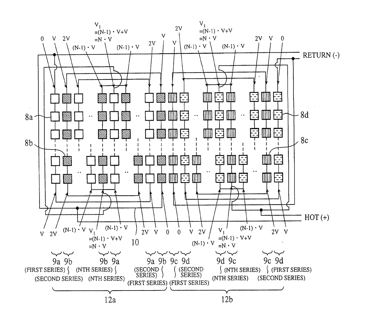
Figure 1 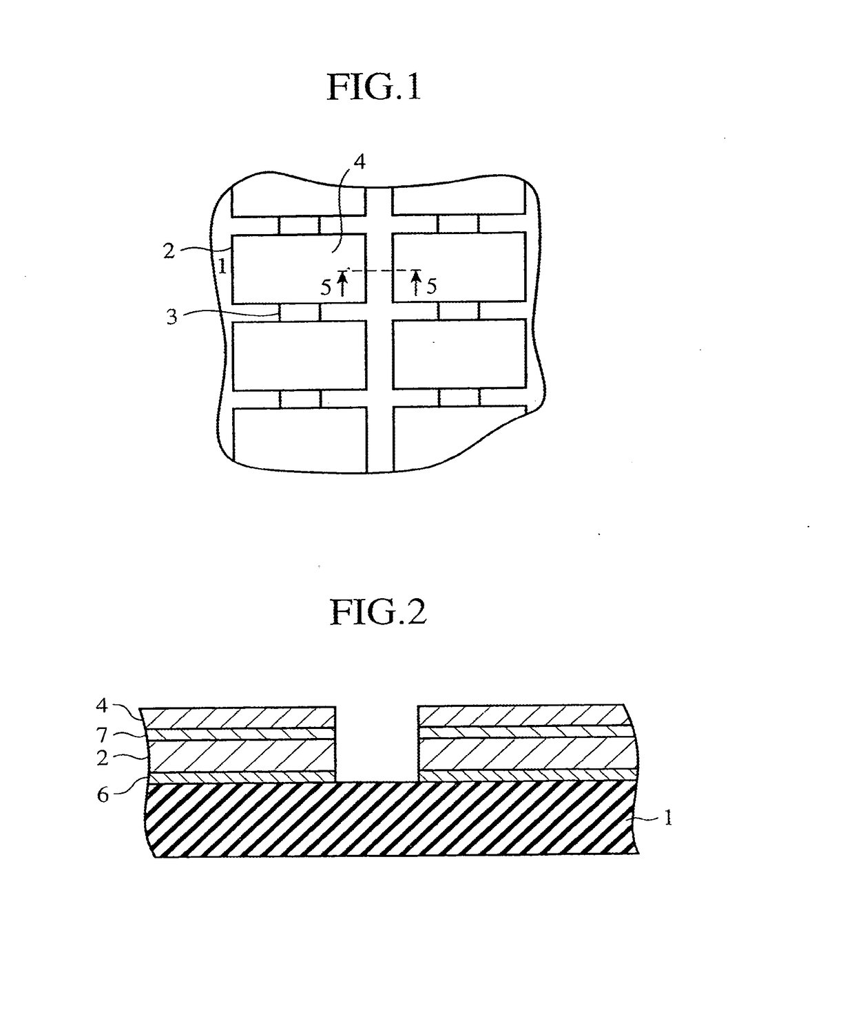
Figure 2 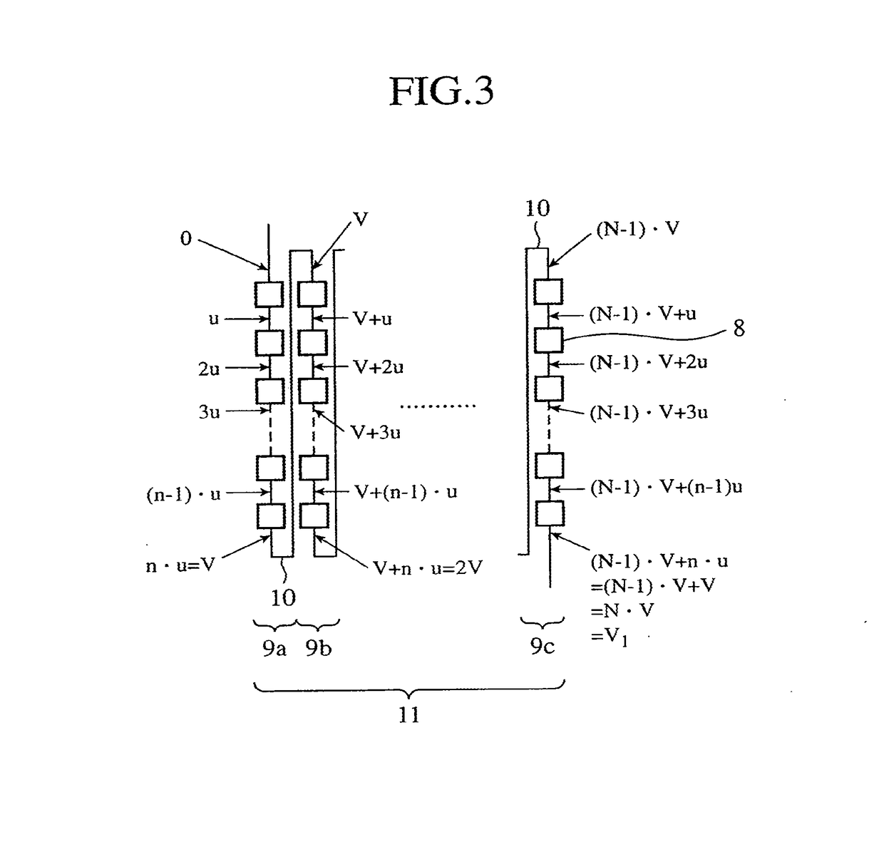
Figure 3
Abstract
Description
CROSS-REFERENCE TO RELATED APPLICATION
[0001] This application is a continuation of U.S. patent application Ser. No. 10 / 508,539, filed Sep. 27, 2004, which is the U.S. National Stage Application of PCT International Application No. PCT / JP04 / 01200, filed Feb. 5, 2004, which claims priority to Japanese Patent Application No. 2003-033735, filed Feb. 12, 2003. The entire contents of each of the above applications are incorporated herein by reference in entirety.Field of the Invention
[0002] The present invention relates to a solar cell panel for use in spacecrafts, such as satellites and airships. More particularly, it relates to a solar cell array and a solar cell panel structure that can prevent electrical discharges from occurring between any solar cells.BACKGROUND OF THE INVENTION
[0003] In the past, many spacecrafts carrying a solar cell panel have been lofted into space. As spacecrafts become more sophisticated in functionality, solar cell panels which can supply high power to spacecraf...
Examples
embodiment 1
[0021]FIG. 1 is a plan view showing embodiment 1 of the present invention. In FIG. 1, solar cells 2 are secured to a surface of an insulator 1. Interconnectors 3 are connected to each of the solar cells 2, and a cover glass 4 is bonded to each of the solar cells 2.
[0022]FIG. 2 is a cross-sectional view showing a cross section of FIG. 1 taken along the line 5-5.
[0023]As shown in FIG. 2, each solar cell 2 is secured to the surface of the insulator 1 by an adhesive 6, and the cover glass 4 is secured to the light receiving surface of each solar cell 2 by an adhesive 7.
[0024]In FIGS. 1 and 2, wiring for connecting among solar cell assembly series is not shown.
[0025]FIG. 3 is a diagram showing the structure of solar cell circuitry according to embodiment 1 of the present invention.
[0026]In FIG. 3, n solar cell assemblies 8 each having a maximum output voltage u are arranged substantially in a line so that each solar cell assembly series 9 is constructed. Each solar cell assembly series 9...
embodiment 2
[0030]FIG. 1 is a plan view showing embodiment 2 of the present invention. FIG. 2 is a cross-sectional view showing a cross section of FIG. 1 taken along the line 5-5.
[0031]FIG. 4 is a diagram showing solar cell circuitry according to embodiment 2 of the present invention.
[0032]In FIG. 4, n solar cell assemblies 8a each having a maximum output voltage u are arranged substantially in a line so that each solar cell assembly series 9a is constructed. Each solar cell assembly series 9a has a maximum output voltage V=n*u.
[0033]Furthermore, N solar cell assembly series 9a are electrically connected in series byway of connection lines 10 so that a solar cell string 11a is constructed. Similarly, n solar cell assemblies 8b each having a maximum output voltage u are arranged substantially in a line so that each solar cell assembly series 9b is constructed. Each solar cell assembly series 9b has a maximum output voltage V=n*u.
[0034]Furthermore, N solar cell assembly series 9b are electrically...
embodiment 3
[0039]FIG. 1 is a plan view showing embodiment 3 of the present invention. FIG. 2 is a cross-sectional view showing a cross section of FIG. 1 taken along the line 5-5.
[0040]FIG. 5 is a diagram showing solar cell circuitry according to embodiment 3 of the present invention.
[0041]In FIG. 5, n solar cell assemblies 8a each having a maximum output voltage u are arranged substantially in a line so that each solar cell assembly series 9a is constructed. Each solar cell assembly series 9a has a maximum output voltage V=n*u. Furthermore, N solar cell assembly series 9a are electrically connected in series by way of connection lines 10 so that a solar cell string 11a is constructed.
[0042]Similarly, n solar cell assemblies 8b each having a maximum output voltage u are arranged substantially in a line so that each solar cell assembly series 9b is constructed. Each solar cell assembly series 9b has a maximum output voltage V=n*u. Furthermore, N solar cell assembly series 9b are electrically con...