
Circuit structure
Patent Information
- Authority / Receiving Office
- US · United States
- Current Assignee / Owner
- Publication Date
- 2018-03-29
Smart Images
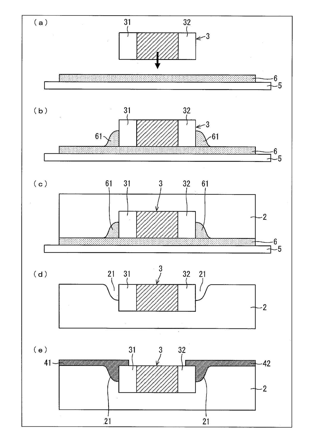
Figure 1 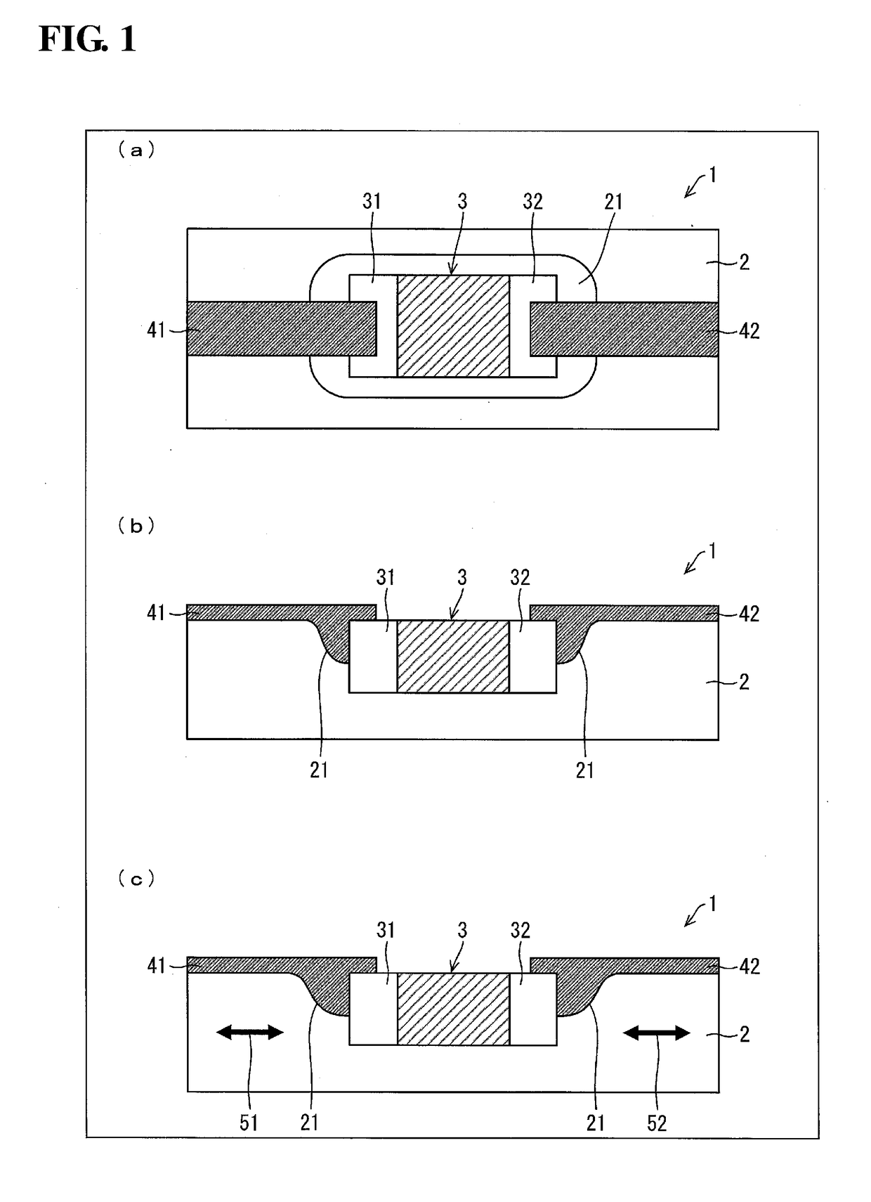
Figure 2 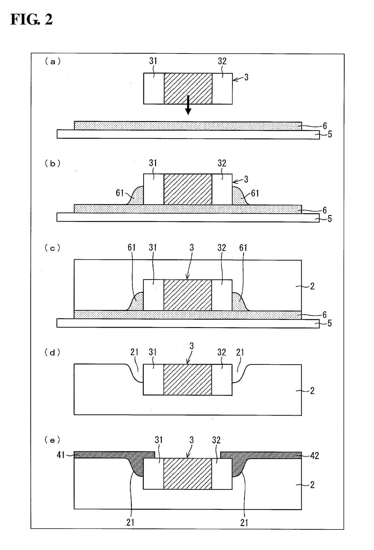
Figure 3
Abstract
Description
TECHNICAL FIELD
[0001] The present invention relates to a circuit structure having a resin molded body in which an electronic component is embedded.RELATED ART
[0002] Recently, demand is on the rise for the realization of thin, light, small, and highly water-resistant wearable products of portable electronic devices, small sensors, health-care devices (electronic thermometers, sphygmomanometers, etc.), and the like at a low cost.
[0003] Typically, such electronic devices are configured by installing passive components (resistances, capacitors, etc.), active components (LSIs, ICs, etc.), power source devices (batteries, etc.), display devices (LEDs, etc.), and other electronic components (sensors, switches, etc.) on printed circuit boards. Conventionally, these printed circuit boards are produced using a method for forming a wiring circuit by etching a copper foil laminated on an epoxy resin board reinforced using glass fibers (glass epoxy board) or on a polyimide sheet (flexible printed b...
Examples
embodiment 1
[0034]Hereinafter, Embodiment 1 of the present invention will be described with reference to FIGS. 1 and 2.
Configuration of Circuit Structure 1
[0035]FIG. 1 is a diagram showing the main configuration of a circuit structure 1 according to Embodiment 1 of the present invention. FIG. 1(a) is a top view of the circuit structure 1, and FIG. 1(b) is a side cross-sectional view of the circuit structure 1. As shown in FIG. 1(a), the circuit structure 1 includes a resin molded body 2, an electronic component 3, and wiring lines 41 and 42.
[0036]The circuit structure 1 is a portion that is to be installed on various devices such as portable electronic devices, small sensors, health-care devices (electronic thermometers, sphygmomanometers, etc.), and the like, and that performs the main or sub functions of the devices. The circuit structure 1 can incorporate a plurality of electronic components 3, and thus the size thereof can be smaller than that of a conventional circuit structure using print...
embodiment 2
[0054]Hereinafter, Embodiment 2 of the present invention will be described with reference to FIGS. 3 and 4. Note that the same constituent elements as those in Embodiment 1 are denoted by the same reference numerals, and a description thereof has been omitted.
Configuration of Circuit Structure 1a
[0055]FIG. 3 is a diagram showing the main configuration of a circuit structure 1a according to Embodiment 2 of the present invention. FIG. 3(a) is a top view of the circuit structure 1a, and FIG. 3(b) is a side cross-sectional view of the circuit structure 1a. As shown in FIG. 3(a), the circuit structure 1a includes the resin molded body 2, the electronic component 3, and the wiring lines 41 and 42, as in the circuit structure 1 according to Embodiment 1 of the present invention. However, the circuit structure 1a according to this embodiment is different from the circuit structure 1 according to Embodiment 1, in that recesses 43 and 44 are respectively formed in the wiring lines 41 and 42....
embodiment 3
[0061]Hereinafter, Embodiment 3 of the present invention will be described with reference to FIG. 5. Note that the same constituent elements as those in Embodiment 1 or 2 are denoted by the same reference numerals, and a description thereof has been omitted.
Configuration of Circuit Structure 1b
[0062]FIG. 5 is a diagram showing the main configuration of a circuit structure 1b according to Embodiment 3 of the present invention. FIG. 5(a) is a top view of the circuit structure 1b, and FIG. 5(b) is a side cross-sectional view of the circuit structure 1b. As shown in FIG. 5(a), the circuit structure 1b includes the resin molded body 2, the electronic component 3, and the wiring lines 41 and 42, as in the circuit structure 1a according to Embodiment 2 of the present invention. Furthermore, as shown in FIG. 5(b), also in the circuit structure 1b according to this embodiment, the recesses 43 and 44 are respectively formed in the wiring lines 41 and 42 as in the circuit structure 1a accordi...