
Active matrix substrate and method for manufacturing the same
Patent Information
- Authority / Receiving Office
- US · United States
- Current Assignee / Owner
- Publication Date
- 2020-03-19
Smart Images
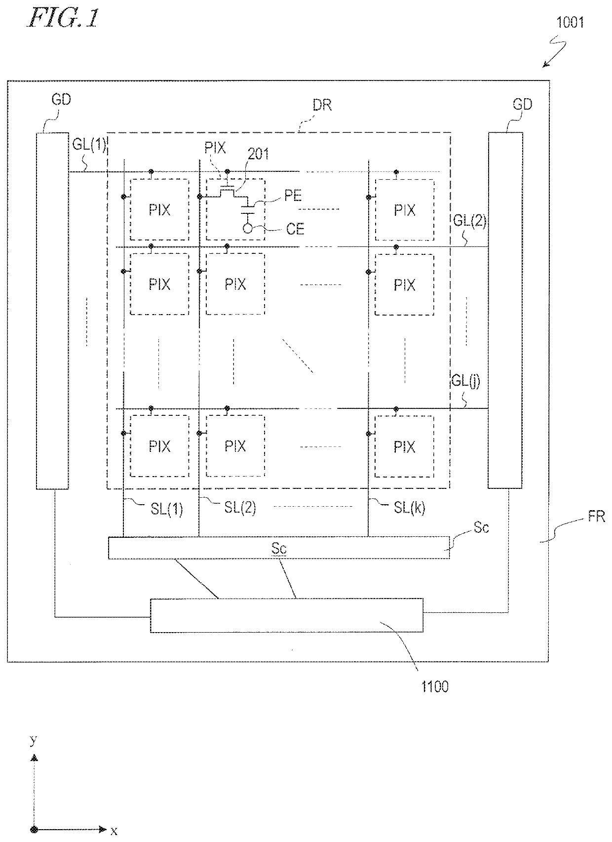
Figure 1 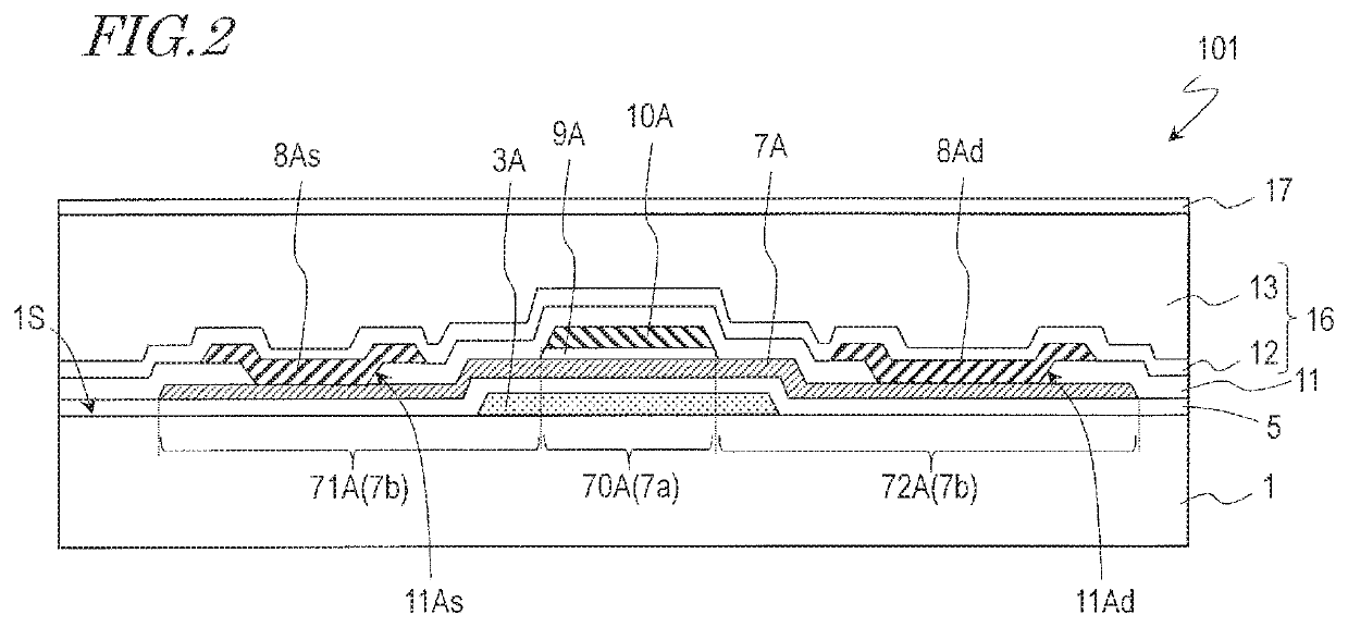
Figure 2 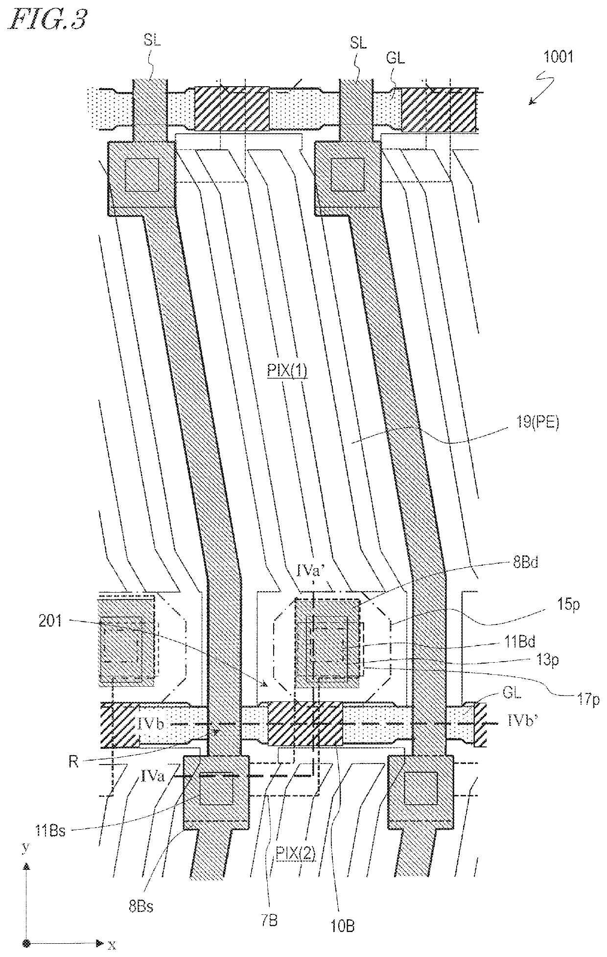
Figure 3
Abstract
Description
[0001] This application claims priority to U.S. Provisional Patent Application No. 62 / 733,268 filed on Sep. 19, 2018, the disclosure of which is incorporated herein by reference.BACKGROUND1. Technical Field
[0002] The present invention relates to an active matrix substrate using an oxide semiconductor and a method for manufacturing the same.2. Description of the Related Art
[0003] Display devices having an active matrix substrate on which a switching element is provided for each pixel have been widely used. An active matrix substrate including thin film transistors (hereinafter “TFTs”) as switching elements is referred to as a TFT substrate. Note that in the present specification, a portion of a TFT substrate that corresponds to a pixel of a display device may also be referred to as a pixel. A TFT provided as a switching element for each pixel of the active matrix substrate is referred to as a “pixel TFT”.
[0004] In recent years, it has been proposed to use an oxide semiconductor as the ma...
Examples
first embodiment
[0076]An active matrix substrate of the first embodiment will now be described with reference to the drawings. An active matrix substrate on which gate driver and source switching (Source Shared driving: SSD) circuits are formed monolithically will be described below as an example. Note that there is no limitation on the active matrix substrate of the present embodiment as long as it has a peripheral circuit that includes at least one circuit TFT monolithically formed thereon.
[0077]FIG. 1 is a schematic diagram showing an example of a planar structure of an active matrix substrate 1001 of the present embodiment.
[0078]The active matrix substrate 1001 includes a display region DR and a region (non-display region or bezel region) FR other than the display region DR. The display region DR includes pixel regions PIX that are arranged in a matrix pattern. The pixel region PIX (which may be referred to simply as a “pixel”) is a region corresponding to a pixel of the display device. The non...
second embodiment
[0186]An active matrix substrate of the second embodiment of the present invention will now be described with reference to the drawings.
[0187]The present embodiment is different from the first embodiment in that the second TFT (pixel TFT) having the bottom gate structure do not include the island-shaped conductor layer 10B.
[0188]FIG. 10 is a schematic cross-sectional view showing a first TFT 102, which is a circuit TFT. FIG. 11 is a plan view illustrating a pixel region PIX of an active matrix substrate 1002 of the present embodiment. FIG. 12 is a schematic cross-sectional view of a second TFT 202, which is a pixel TFT, showing a cross-sectional structure taken along line XII-XII′ of FIG. 11. Like elements to those of FIGS. 2 to 4B are denoted by like reference numerals. Like elements to those of the embodiment described above may not be further described below.
[0189]The first TFT 102 is a top gate structure or double gate structure TFT having a similar configuration to that of the ...
third embodiment
[0215]The active matrix substrate of the present embodiment is different from the embodiment described above in that a further insulating layer is arranged in the intersection between the source bus line SL and the gate bus line GL.
[0216]FIG. 15A and FIG. 15B are a plan view and a cross-sectional view taken along line XVb-XVb′, respectively, showing a portion of a pixel region PIX of the present embodiment.
[0217]In the intersection R1 between the source bus line SL and the gate bus line GL, another island-shaped insulator layer (referred to also as the second island-shaped insulator layer) 9R and another island-shaped conductor layer (referred to also as the second island-shaped conductor layer) 10R are arranged between the lower insulating layer 5 and the upper insulating layer 11. The second island-shaped insulator layer 9R is formed by using the same insulating film as the gate insulating layer 9A and the island-shaped insulator layer 9B. The second island-shaped conductor layer ...