
Display panel
Patent Information
- Authority / Receiving Office
- US · United States
- Current Assignee / Owner
- Publication Date
- 2021-02-18
- Estimated Expiration
- Not applicable · inactive patent
Smart Images
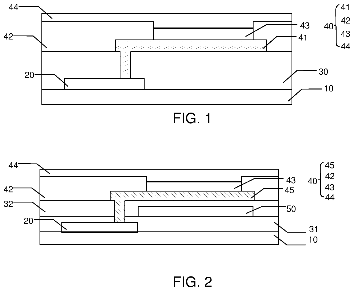
Figure 1
Abstract
Description
FIELD OF INVENTION
[0001] The present disclosure relates to the field of electronic display technologies, and more particularly to a display panel.BACKGROUND OF INVENTION
[0002] Organic light emitting diode (OLED) display panels are widely used in mobile phone screens, displays, and full-color televisions (TVs) because of their self-illumination, high brightness, wide viewing angles, high contrast, flexibility, and low power consumption.
[0003] Anode of a top emitting OLED structure generally adopts a laminated structure composed of indium tin oxide (ITO) and silver (Ag). In order to match the anode to energy levels of an organic light emitting material layer, material in which the anode is in direct contact with an organic material is ITO. In addition, since the anode needs to be used as a reflective electrode, the anode also needs to be provided with metal having high reflectivity for reflection, such as Ag.
[0004] However, Ag is easily oxidized in air to form silver oxide bumps, which ca...
Examples
Embodiment Construction
[0019]The following description of the various embodiments is provided to illustrate the specific embodiments of the present invention. The directional terms mentioned in the present application, such as up, down, front, back, left, right, inside, outside, side, etc., are only directions referring to the additional drawings. Therefore, the directional terminology used is for the purpose of illustration and understanding and is not intended to be limiting. In the figures, structurally similar elements are denoted by the same reference numerals.
[0020]First, the prior art will be briefly described.
[0021]Referring to FIG. 1, FIG. 1 is a schematic structural view of a display panel in the prior art. The display panel is a top emitting display panel, that is, a light emitting surface of the display panel is a surface of a cathode of a light emitting structure that is away from an anode.
[0022]Referring to FIG. 1, the display panel of the prior art includes a substrate 10, a thin film trans...