
Nano-wall Integrated Circuit Structure with High Integrated Density
a technology of integrated circuits and nano-walls, applied in the field of microelectronics technology and integrated circuits, can solve the problems of reducing integration, limiting the improvement of integration, and increasing the area of integrated circuits, so as to increase the driving capability of transistors, reduce the on-resistance ron, and reduce the effect of integration
Patent Information
- Authority / Receiving Office
- US · United States
- Patent Type
- Applications(United States)
- Current Assignee / Owner
- Publication Date
- 2022-05-12
Smart Images
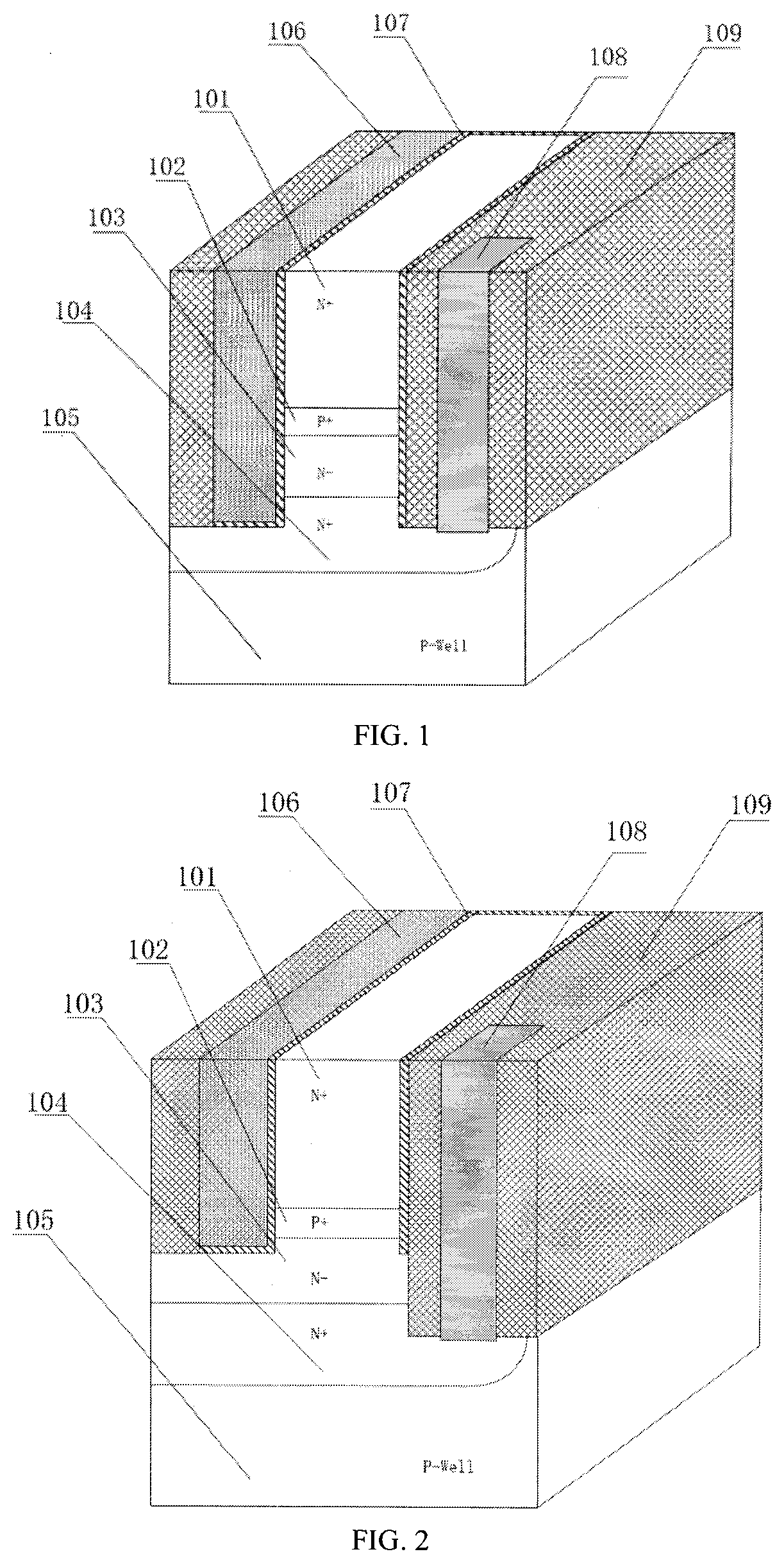
Figure 1 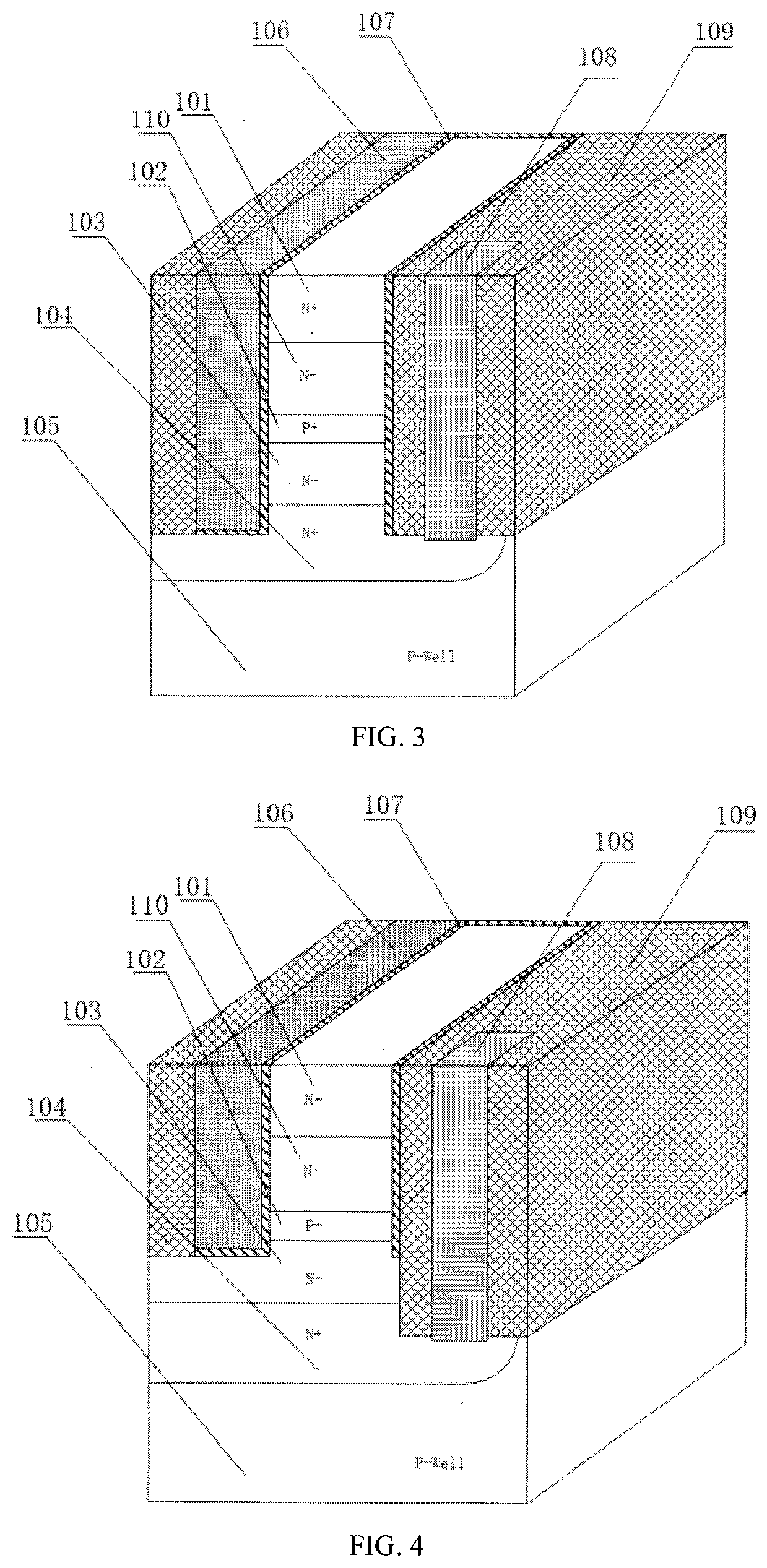
Figure 2 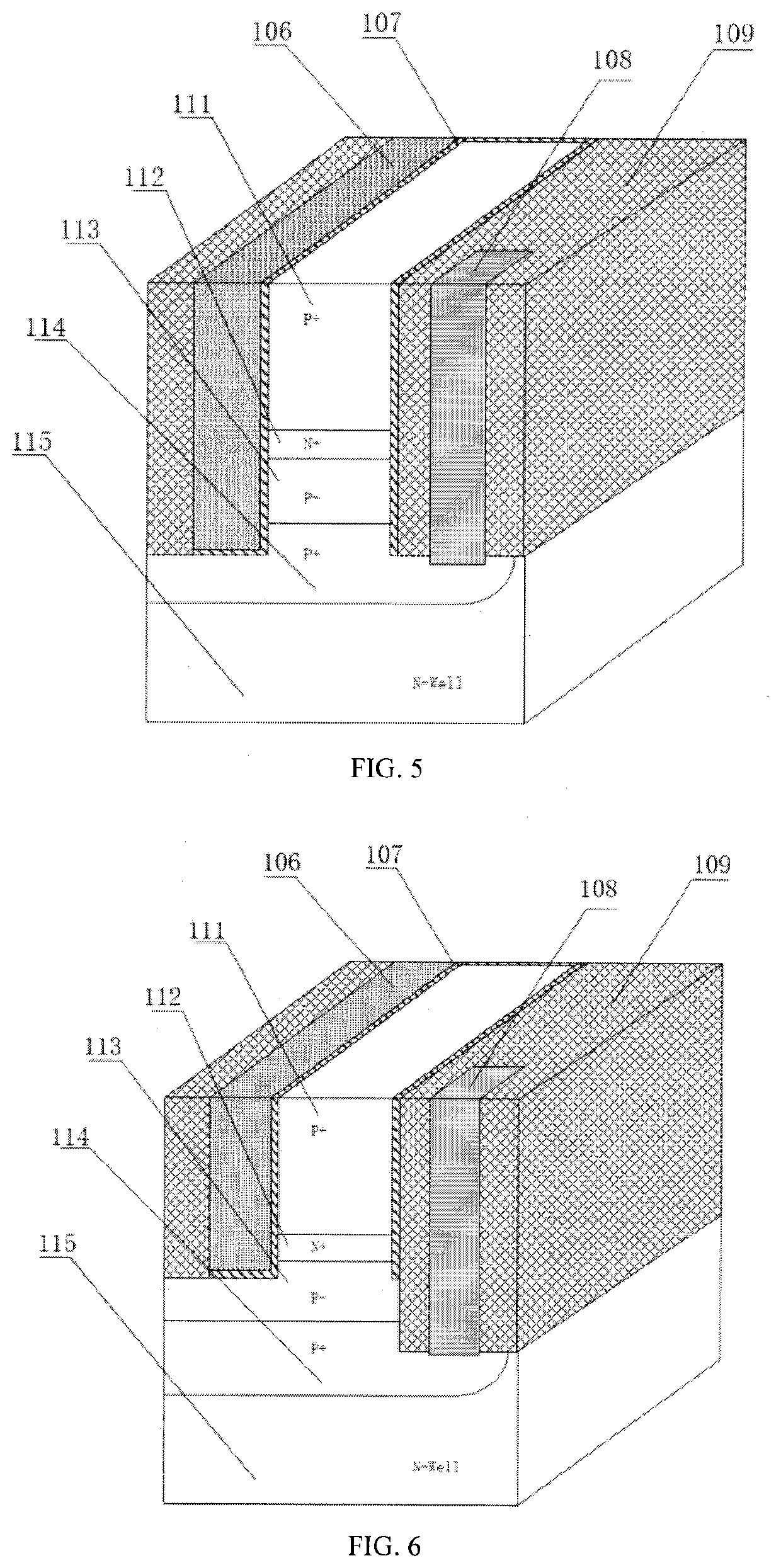
Figure 3
Abstract
Description
TECHNICAL FIELD
[0001] The invention relates to the field of microelectronics technology and integrated circuits.BACKGROUND TECHNIQUE
[0002] The traditional planar MOSFET structure after 22 nm was gradually replaced by the three-dimensional FINFET. FINFET was formally published in a paper by Professor Hu Chenming of the University of California, Berkeley in 2000; the channel region of FINFET is a fin-shaped semiconductor wrapped on three sides of the gate. The three-sided gate structure enhances the gate control ability and effectively suppresses the short channel effect, and allows the continuation of Moore's law. Following the idea of FINFET's three-sided gate structure, after the 5 nm node, people proposed a four-sided gate structure GAAFET (Gate-All-Around Field Effect Transistor) structure.
[0003] MOSFET is divided into N-type and P-type. N-type carriers are electrons, P-type carriers are holes, and the electron mobility is about 3 times the hole mobility. Therefore, in the CMOS proc...
Examples
example 1
[0053]A computer three-dimensional simulation was performed based on the CMOS inverter structure using the technical embodiments 6 and 8 of this invention, and the simulation structure is shown in FIG. 14. For the NMOSFET, the N+ heavily doped source region is silicon, the depth or thickness is 20 nm, and the doping concentration is 1×1020 cm−3. The depth or thickness of the N− lightly doped source region is 20 nm, and the doping concentration is 1×1016 cm−3. The depth or thickness of the P+ channel region is 10 nm, and the doping concentration is 1×1018 cm−3. The depth or thickness of the N− lightly doped drain region is 20 nm, and the doping concentration is 1×1016 cm−3. The depth or thickness of the N+ heavily doped drain region is 20 nm, and the doping concentration is 1×1020 cm−3. For the PMOSFET, the depth or thickness of the P+ heavily doped source region is 20 nm, and the doping concentration is 1×1020 cm−3. The depth or thickness of the P− lightly doped source region is 20 ...
example 2
[0055]A computer three-dimensional simulation was performed based on the NMOSFET structure using the technical embodiment 4 of this invention, and the cross-sectional view of the simulation structure is shown in FIG. 16. The N+ heavily doped source region material is silicon, the depth or thickness is 10 nm, and the doping concentration is 1×1020 cm−3. The depth or thickness of the N− lightly doped source region is 20 nm, and the doping concentration is 1×1017 cm−3. The depth or thickness of the P+ channel is 0.543 nm, and the doping concentration is 2×1020 cm−3. The depth or thickness of the N− lightly doped drain region is 20 nm, and the doping concentration is 1×1017 cm−3. The depth or thickness of the N+ heavily doped drain region is 10 nm, and the doping concentration is 1×1020 cm−3. The gate material is polysilicon, and the depth is 2 nm below the bottom surface of the P+ channel region. The gate dielectric material is silicon dioxide with a thickness of 1.1 nm. The gate is ar...
example 3
[0057]A computer three-dimensional simulation was performed based on the NMOSFET structure using the technical embodiment 2 of this invention, and the cross-sectional view of the simulation structure is shown in FIG. 20. The N+ heavily doped source region material is SiGe, the depth or thickness is 10 nm, and the doping concentration is 1×1020 cm−3. The depth or thickness of the P+ channel is 7 nm, and the doping concentration is 5×1019 cm−3. The depth or thickness of the N− lightly doped drain region is 10 nm, and the doping concentration is 1×1015 cm−3. The depth or thickness of the N+ heavily doped drain region is 10 nm, and the doping concentration is 1×1020 cm−3. The gate material is polysilicon, and the depth is flush with the bottom surface of the P+ channel region. The gate dielectric material is silicon dioxide, and the thickness is 2 nm. The gate is arranged on three sides of the PN functional area, the corresponding channel width is 21 nm, and the channel width-to-length ...