
Carbon-doped silicon single crystal wafer and method for manufacturing the same
Patent Information
- Authority / Receiving Office
- US · United States
- Current Assignee / Owner
- Publication Date
- 2022-08-18
Smart Images
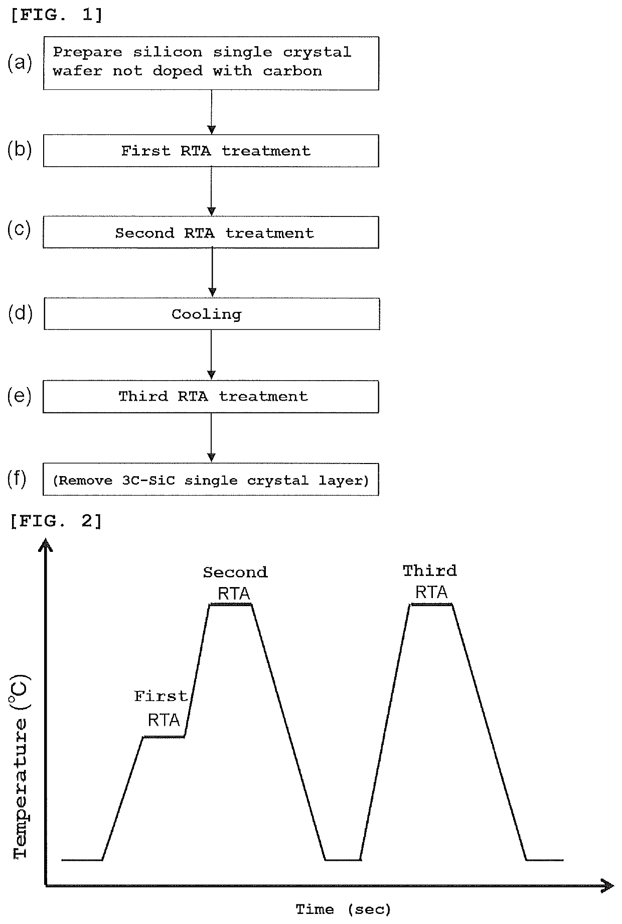
Figure 1 
Figure 2
Abstract
Description
TECHNICAL FIELD
[0001] The present invention relates to a carbon-doped silicon single crystal wafer and a method for manufacturing the carbon-doped silicon single crystal wafer.BACKGROUND ART
[0002] Silicon single crystal wafers are widely employed as substrates for manufacturing semiconductor devices. Meanwhile, for gettering metal impurities which enter as contaminants during the semiconductor-device manufacturing process, it is well known that silicon single crystal wafers are provided with gettering ability. By the way, cutting-edge devices have been manufactured under lower temperature conditions recently. Silicon single crystal wafers doped with carbon have been employed which promotes BMD (Bulk Micro Defects) formation by oxygen precipitation even in low temperature processes because the resultant serves as gettering sites of metal impurities in manufacturing processes.
[0003] Moreover, it is also well known that silicon single crystal wafers are doped with nitrogen or carbon to en...
Examples
example
[0100]First, a silicon single crystal ingot was pulled according to Czochralski method, and a wafer was processed therefrom. Thus, as a silicon single crystal wafer not doped with carbon, a silicon single crystal wafer was prepared (step a) which had a diameter of 200 mm, crystal plane orientation (100), P type, normal resistance, oxygen concentration of 12 ppma (JEITA), carbon concentration of less than 2.5×10¹⁵ atoms / cm3, and Nv region as defect region.
[0101]Next, the first, second, and third RTA treatments were performed as follows.
[0102]After the silicon single crystal wafer was put in an RTA treatment apparatus, the temperature was raised from room temperature to 800° C. Then, the temperature was maintained at 800° C. for 20 seconds (step b, first RTA). In this event, the atmosphere was CH4+H2 / Ar with 2% carbon concentration.
[0103]Next, the temperature was raised to 1200° C., and maintained at 1200° C. for 10 seconds (step c, second RTA). In this event, the atmosphere was CH4+H...