
Gain cell type non-volatile memory having charge accumulating region charged or discharged by channel current from a thin film channel path
a non-volatile memory and channel current technology, applied in semiconductor devices, solid-state devices, instruments, etc., can solve the problems of increasing leak current flow, narrowing the depletion layer width, and increasing the density of the substrate, so as to reduce the leak current
Patent Information
- Authority / Receiving Office
- US · United States
- Current Assignee / Owner
- Publication Date
- 2005-04-05
- Estimated Expiration
- Not applicable · inactive patent
Smart Images
Figure 1 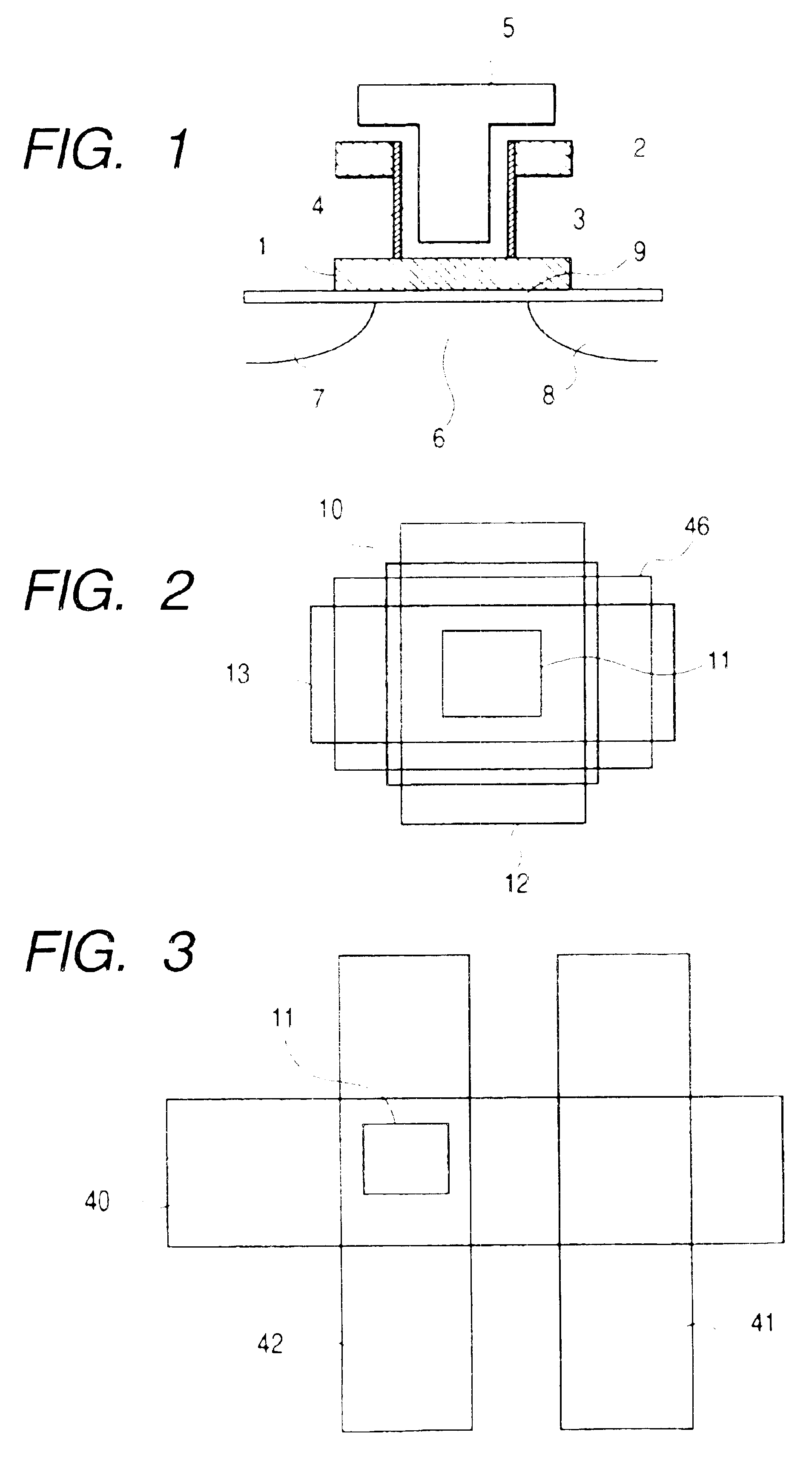
Figure 2 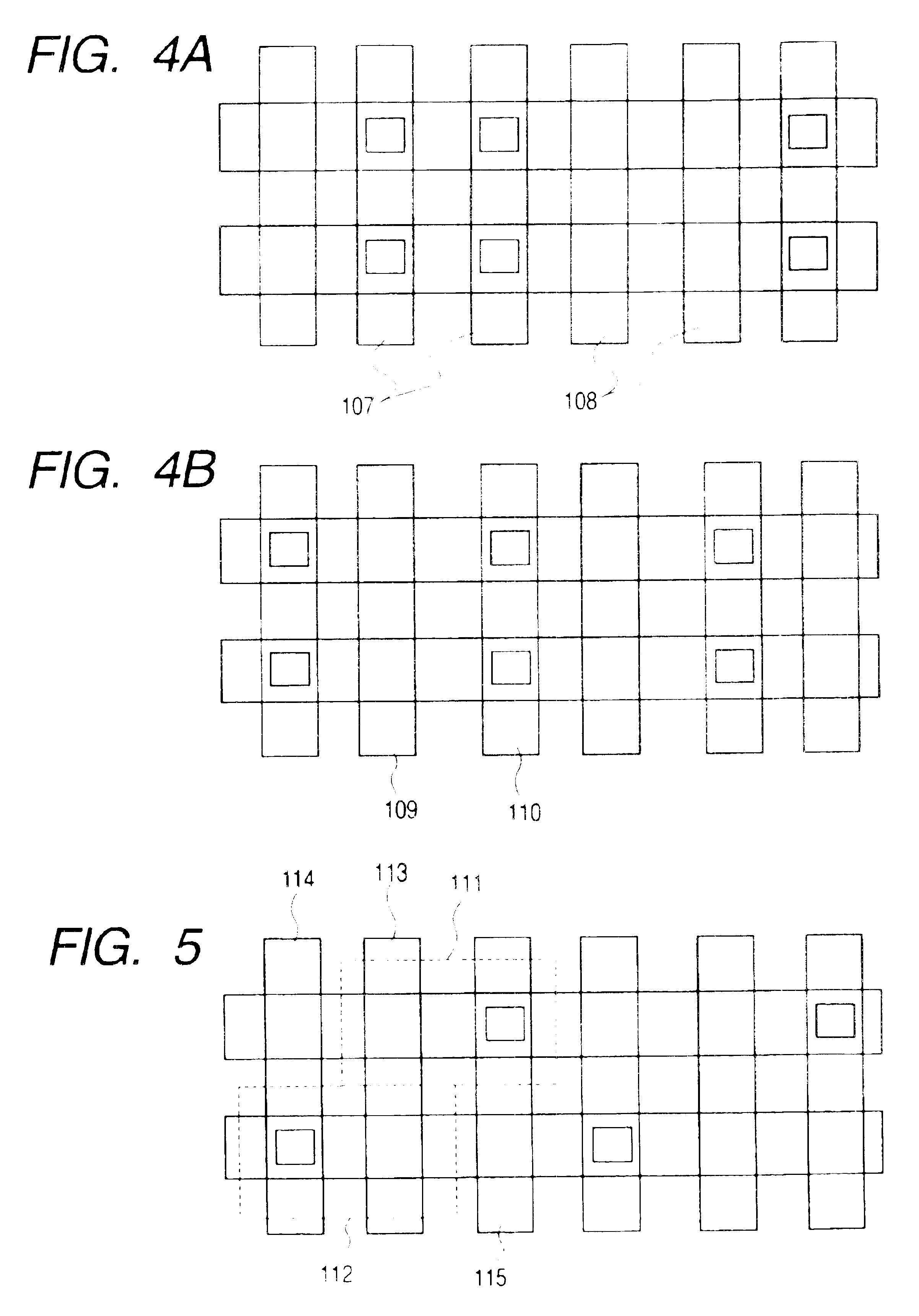
Figure 3
Abstract
Description
BACKGROUND OF THE INVENTION1. Field of the InventionThe present invention relates to a semiconductor element and a semiconductor device.2. Description of the Related ArtMOSFETs (metal-oxide-semiconductor field effect transistors) are normally placed in an off-state to prevent currents from leaking by means of pn junctions. The primary causes of leak currents include subthreshold currents and reversed carrier recombination. Such currents are small but not negligible; they determine the data holding time of DRAMs (dynamic random access memories) and define their refresh cycles. Schemes proposed so far to minimize leak currents include the reduction of crystal defects with wafers subject to epitaxial growth, and complete depletion in the off-state by use of SOI (silicon on insulator) wafers.There has been proposed a memory element structure called gain cells capable of operating as DRAM cells with reduced stored charges. The proposed structure involves electrically charging a memory no...
Examples
first embodiment
Semiconductor elements and semiconductor devices specifically embodying the invention are described below. FIG. 23 is a cross-sectional view of a semiconductor element practiced as the first embodiment of the invention. Using an SOI substrate, the semiconductor element includes a source region 300, a drain region 201 and a channel 202 made of single crystal and deposited on an SiO2 film 204. The source 200 and drain 201 are n-type regions of high impurity density. The channel 202 is a p-type channel 4 nm in average thickness, thinner than the source 200 or drain 201 region. A control electrode 203 is constituted by n-type polycrystal silicon of high impurity density. The channel 202 is isolated from the control electrode 203 by a gate insulating film 205 composed of an SiO2 film.
The first embodiment is the same as the common n-channel MOS in that application of a positive voltage to the control electrode 203 turns on the transistor to permit a current flow between the source 200 and...
second embodiment
FIGS. 26A and 26B show a semiconductor element practiced as the second embodiment of the invention. FIG. 26A is a cross-sectional view of the semiconductor element. Unlike the first embodiment that had the source 200, drain 201 and channel 202 formed on the SOI substrate surface, the second embodiment has a source 208, a drain 209 and a channel 210 formed by polycrystal silicon deposited on an, SiO2 layer 214. The source 208 and drain 209 are n-type regions of high impurity density. The channel 210 is made of a non-doped polycrystal silicon film 3 nm in average thickness. The channel portion is deposited in an amorphous state and crystallized later by a heating process. As opposed to the first embodiment in which a thicker silicon film was thinned down to form the channel, the second embodiment need only have a thin film deposited for channel formation and thus entails simpler fabrication processes. The second embodiment is equivalent to the first embodiment in that all channels are...
third embodiment
FIGS. 27A and 27B depict a memory cell structure of a semiconductor memory device practiced as the third embodiment of the invention. FIGS. 27A and 27B are a cross-sectional view and a circuit diagram of the memory cell structure respectively. The transistor of the first embodiment is used as a switching transistor 216 of a DRAM as the third embodiment. Generally, the DRAM retains data by accumulating electrical charges in each of its capacitors 215. The charges gradually dissipate in the form of leak currents through the switching transistor. To hold its data, today's common DRAM has its charges refreshed in cycles of slightly less than one second. The third embodiment affords a prolonged refresh cycle because of reduced leak currents through transistors. That in turn lowers the refresh frequency and decreases power dissipation for data retention. At the same time, the frequency of contention between access and refresh operations is also lowered, which reduces the average access ti...