
Charge pump device
a charge pump and pump body technology, applied in semiconductor devices, dc-dc conversion, power conversion systems, etc., can solve the problems of reducing the resistance of the charge transfer mos, latching, and drawing harmonic noise when switching a current, so as to reduce the resistance of the well region, suppress the back gate bias effect of the mos transistor, and reduce the effect of the well region resistan
Patent Information
- Authority / Receiving Office
- US · United States
- Patent Type
- Patents(United States)
- Current Assignee / Owner
- Publication Date
- 2005-08-09
- Estimated Expiration
- Not applicable · inactive patent
Smart Images
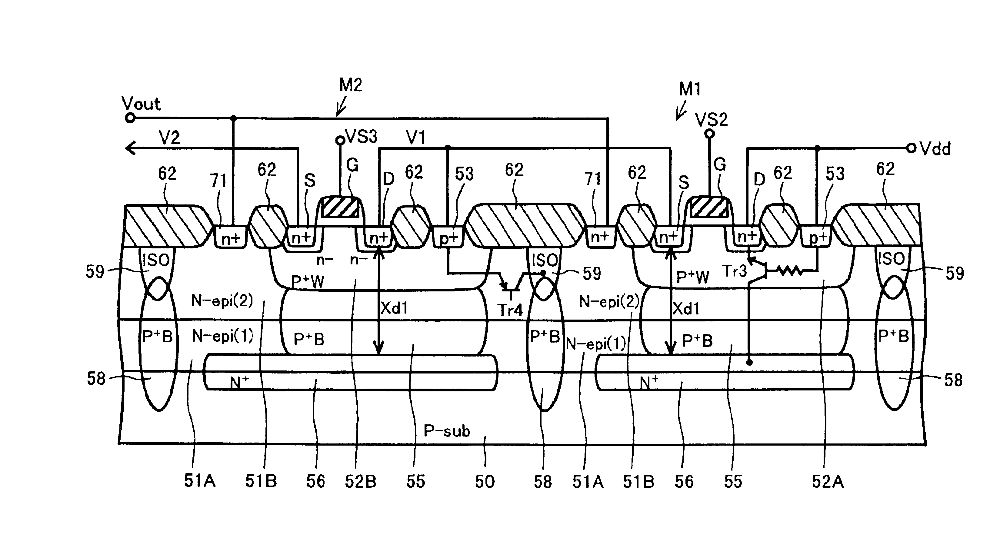
Figure 1 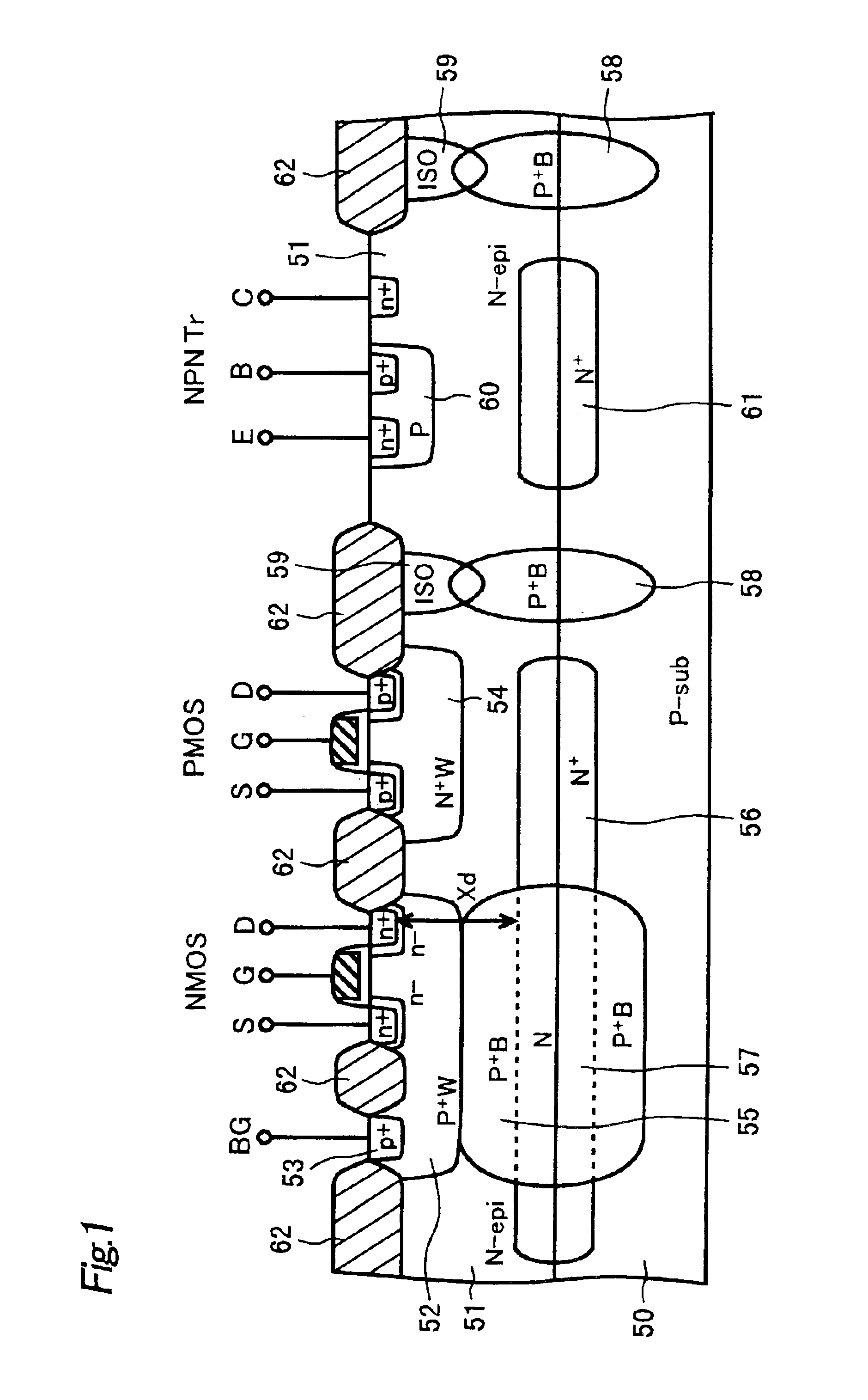
Figure 2 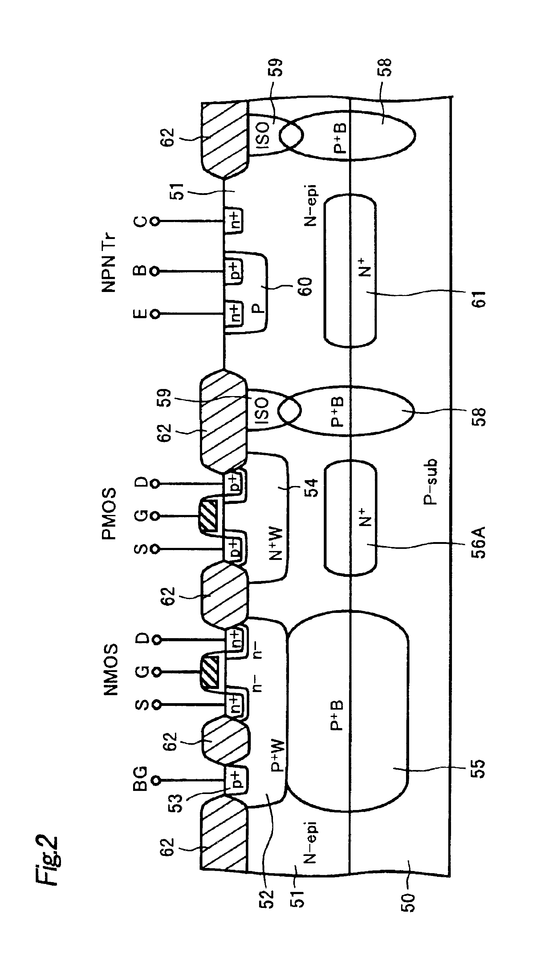
Figure 3
Abstract
Description
BACKGROUND OF THE INVENTION
[0001] 1. Field of the Invention
[0002] This invention relates to a semiconductor device and its manufacturing method, specifically to a charge pump device with large current capacity used for a power supply circuit. Performance of the charge pump device can be improved and a latch up can be prevented with this invention.
[0003] 2. Description of the Related Art
[0004] Video equipment in recent years such as a camcorder, a digital still camera (DSC) and a mobile phone with DSC use CCDs (charge-coupled devices) to capture an image. A CCD drive circuit for driving the CCDs requires a power supply circuit that provides both positive and negative high voltages (over 10 volts) and a large current (several milliamperes). A switching regulator is used for that purpose today
[0005] The switching regulator can generate a high voltage with high performance, i.e. with high power efficiency (output power / input power). However, it has a drawback to generate a harmonic noise whe...
Examples
first embodiment
[0059]Next, this invention will be explained referring to FIGS. 1-4. First, a structure of a BiCMOS device, with which a charge pump device is implemented in an integrated circuit, will be explained referring to FIG. 1.
[0060]Each of an N-channel MOS transistor (NMOS), P-channel transistor (PMOS) and an NPN bipolar transistor (NPN Tr) is formed in each of predetermined regions in an N-type epitaxial silicon layer 51, having resistivity of 1.25 Ωcm, for example, grown by vapor phase epitaxy on a P-type single crystalline silicon substrate 50.
[0061]The N-channel MOS transistor is formed in a P-type well region 52 formed in a surface of the N-type epitaxial silicon layer 51. The P-type well region 52 is, for example, about 2 μm deep. The N-channel MOS transistor has an N+-type drain layer D, an N+-type source layer S, both formed in the surface of the P-type well region 52, and a gate electrode G formed on a gate insulation film. The N-channel MOS transistor can be formed in a so-called...
second embodiment
[0090]FIG. 5 is a cross-sectional view showing a charge pump device according to this invention.
[0091]Circuit structure of this charge pump device is similar to that of the first embodiment. The charge transfer MOS transistors M2 and M3 of the charge pump device of FIG. 19 are shown in FIG. 5, as in the case of the first embodiment.
[0092]Difference from the first embodiment is that the P+-type buried layer 55 is not formed below the P-type well regions 52A and 52B. Although the effect to reduce the resistance of the P-type well regions 52A and 52B is lost because of the lack of the P+-type buried layer 55, it seems that robustness against latch up is increased compared with the conventional charge pump device by adding the lower isolation layer 58 and the upper isolation layer 59.
third embodiment
[0093]FIG. 6 is a cross-sectional view showing a charge pump device according to this invention.
[0094]Circuit structure of this charge pump device is similar to that of the first embodiment. The charge transfer MOS transistors M2 and M3 of the charge pump device of FIG. 19 are shown in FIG. 6.
[0095]Difference from the first embodiment is that neither the N+-type buried layer 56 nor the P+-type buried layer 55 is formed below the P-type well regions 52A and 52B.
[0096]Although the effect to reduce the resistance of the N-type epitaxial silicon layers 51 is lost because of the lack of the N+-type buried layer 56, it seems that robustness against latch up is increased compared with the conventional charge pump device by adding the lower isolation layer 58 and the upper isolation layer 59.
[0097]Next, a fourth embodiment of this invention will be explained referring to FIGS. 7-17. In the charge pump device of this embodiment, a voltage from a level shift circuit is applied to a gate of a ...