
Staggered wirebonding configuration
a wirebonding configuration and finger technology, applied in the direction of electrical equipment, semiconductor devices, semiconductor/solid-state device details, etc., can solve the problem of confined pitch of the bonding pad, achieve the effect of reducing the cost of the chip package, increasing the number of bonding pads, and enhancing chip efficiency
Patent Information
- Authority / Receiving Office
- US · United States
- Patent Type
- Patents(United States)
- Current Assignee / Owner
- Publication Date
- 2008-08-12
Smart Images
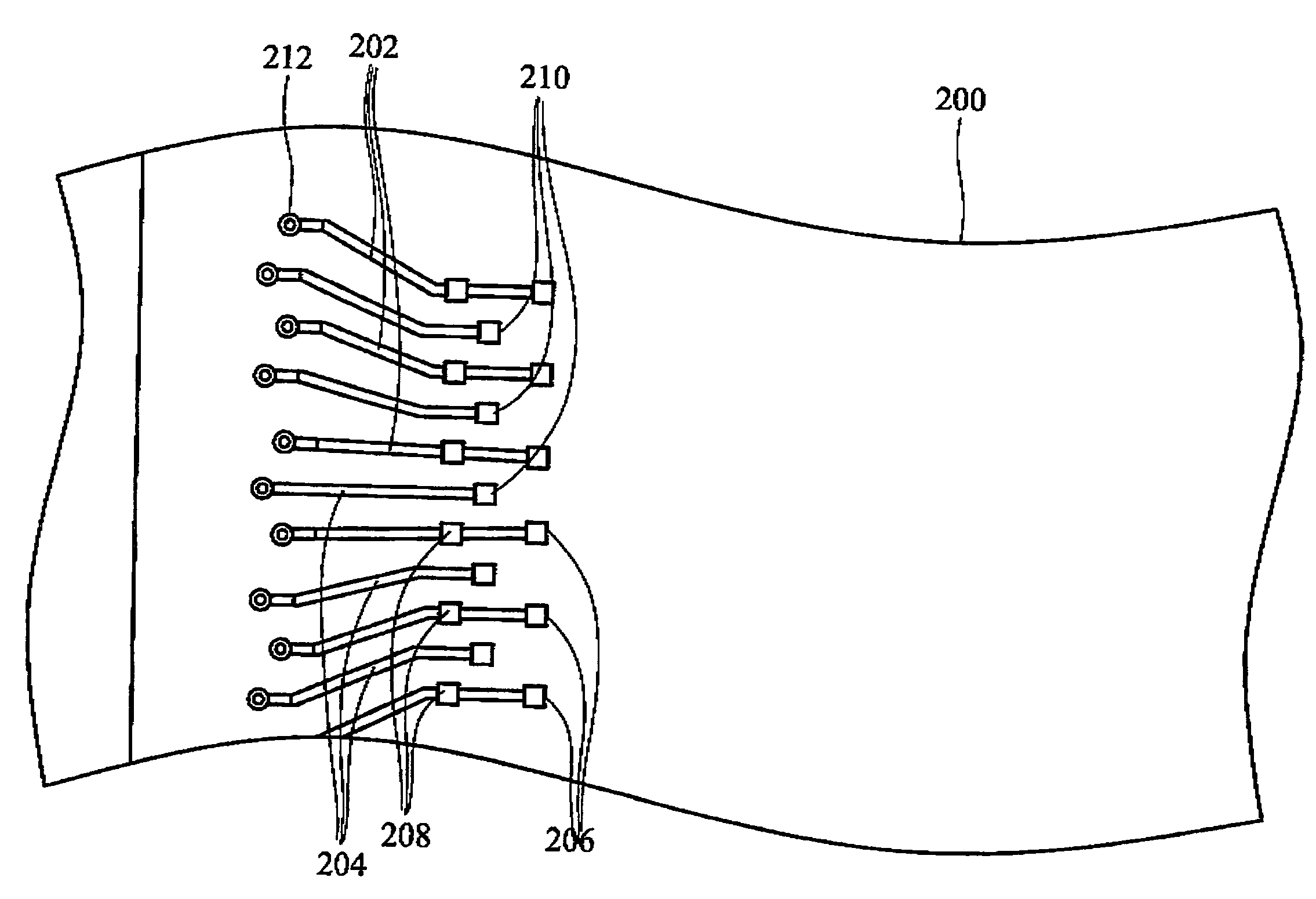
Figure 1 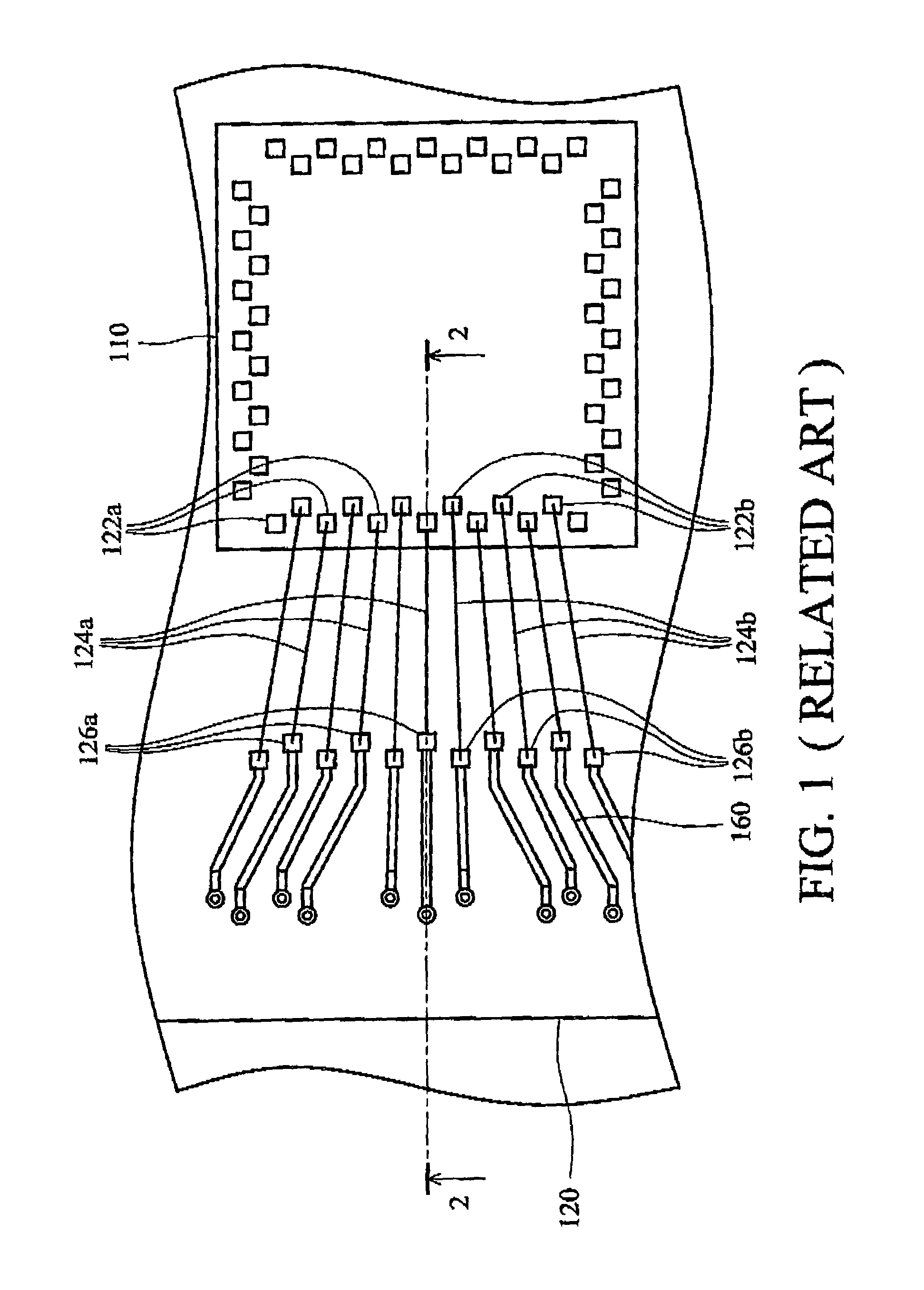
Figure 2 
Figure 3
Abstract
Description
[0001] This application claims foreign priority under 35 USC 119 of Taiwan Application Serial No. 093133828, filed May 11, 2004, which is hereby incorporated by reference.BACKGROUND
[0002] The present invention relates in general to a staggered finger configuration and more particularly to a staggered finger configuration for chips with staggered bonding pads.
[0003] As the efficiency and complexity of semiconductor chips increase, semiconductor packages provide increased efficiency.
[0004] In wire bonding, the arrangement of bonding pads on a chip is important. In a package process such as ball grid array (BGA), the pitch of conductive wires on a substrate can be very small due to photolithography technique. Nevertheless, the pitch of the bonding pads is confined by the design rule of wire bonding process, remaining unable to scale down to match the conductive wires. As a result, the arrangement of bonding pads has become a critical parameter in package efficiency.
[0005] Generally, the num...
Examples
Embodiment Construction
[0025]FIG. 4 is a top view of a substrate bearing a staggered finger configuration according to an embodiment of the invention. In this embodiment, a substrate 200 has a plurality of first and second conductive wires arranged alternately thereon. Each of the first conductive wires connects to a pair of inner and an outer finger 206, 208, and each of the second conductive wires connects to an intermediate finger between the inner and outer fingers 206, 208, providing a staggered finger configuration connecting to signal pads on the chip. The substrate 200 may be a core substrate with vias, blind vias or buried vias. Additionally, the substrate 200 and the first and the second conductive wires 202, 204 further comprise a solder mask 24030 thereon (as shown in FIG. 7). The fingers 206, 208, and 210 are exposed under openings of the solder mask 240. In this embodiment, the openings may be rectangular or other shape such as square, circular or polygonal.
[0026]Again referring to FIG. 4, t...