
Microelectric programmable device and methods of forming and programming the same
a microelectronic and programmable technology, applied in the direction of instruments, visual presentation using printers, transistors, etc., can solve the problems of increasing the voltage required to reduce the resistance of the device, and achieve the effect of reducing the cross-sectional area of the interface, increasing the efficiency of the device, and reducing the interface area
Patent Information
- Authority / Receiving Office
- US · United States
- Patent Type
- Patents(United States)
- Current Assignee / Owner
- Publication Date
- 2010-03-09
- Estimated Expiration
- Not applicable · inactive patent
Smart Images
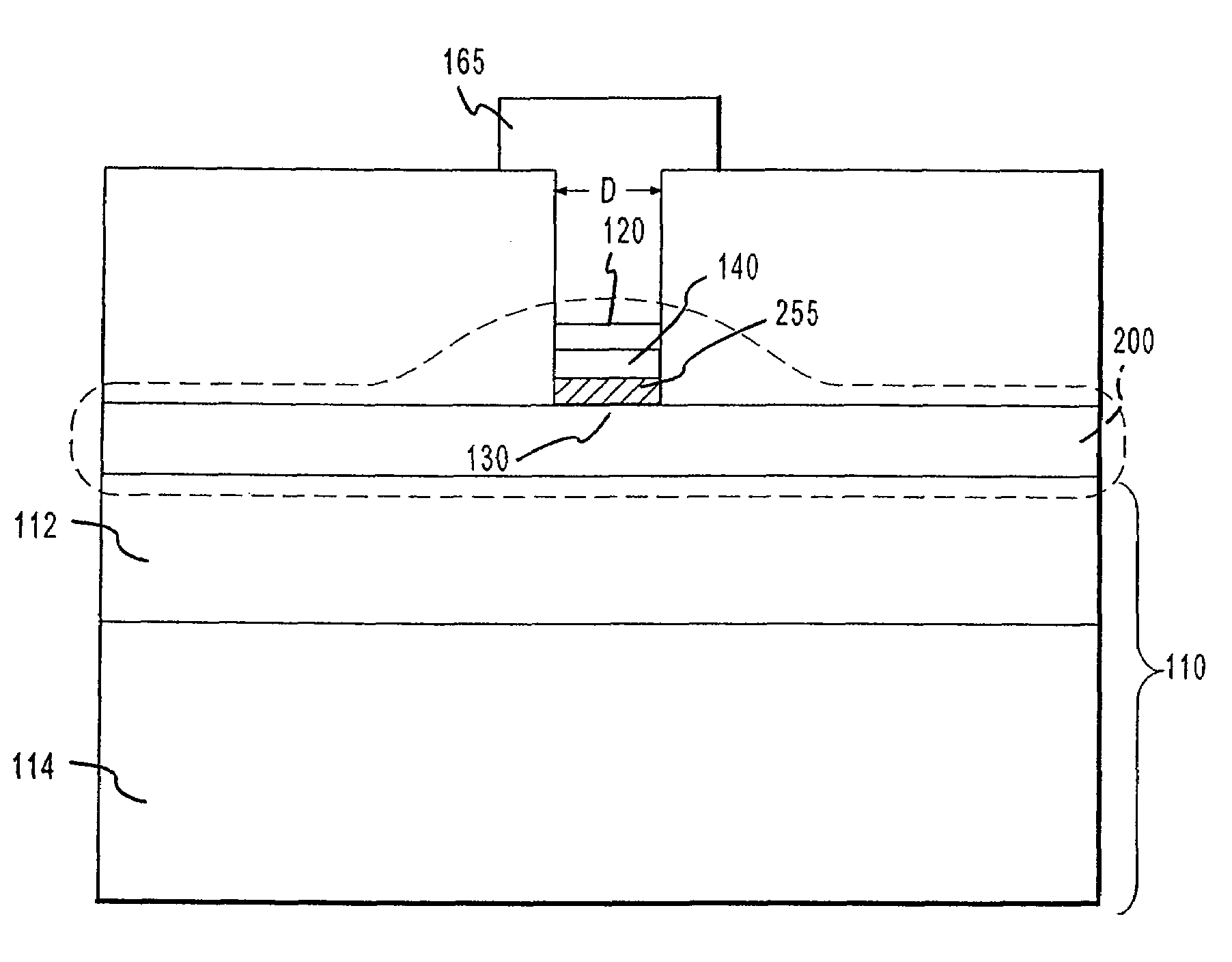
Figure 1 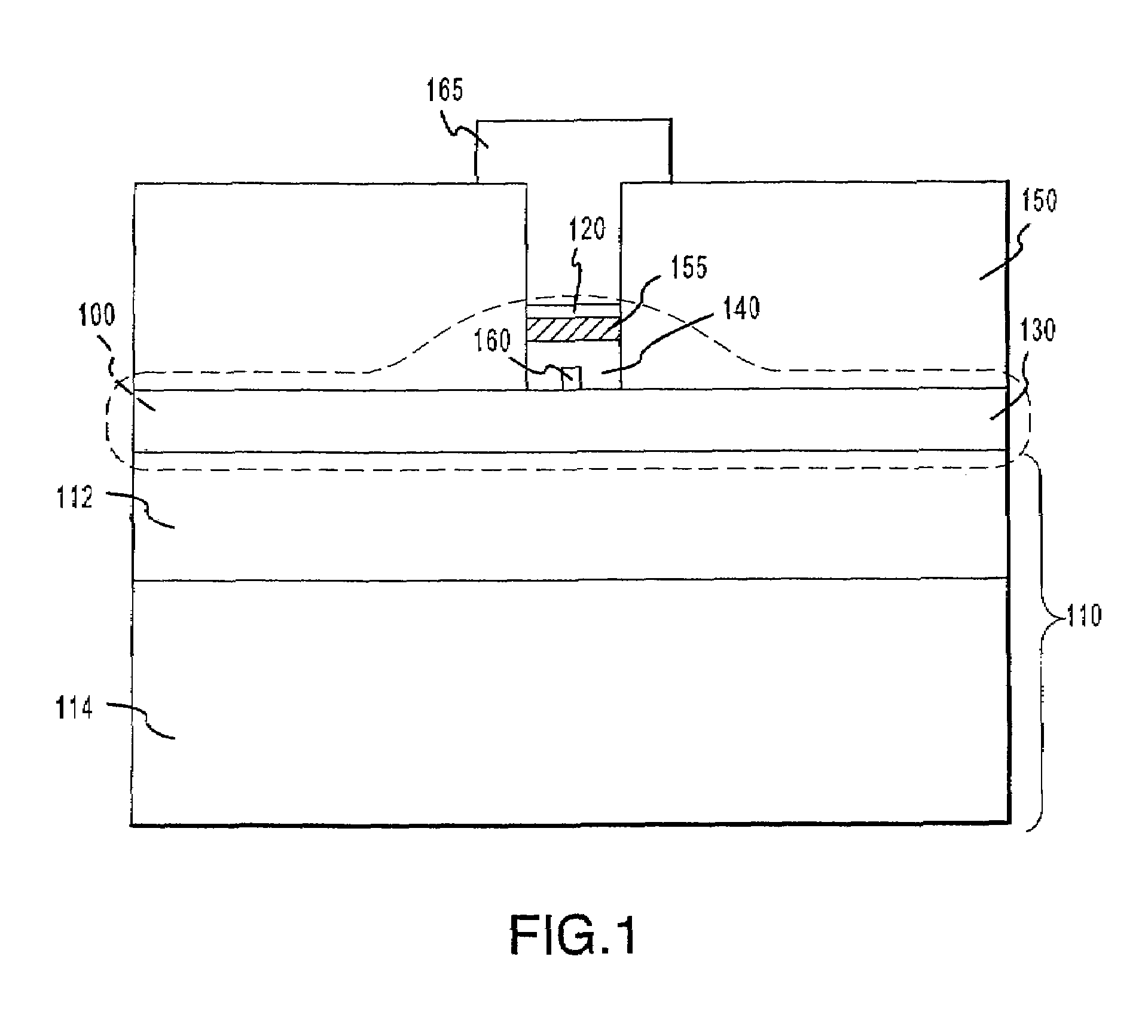
Figure 2 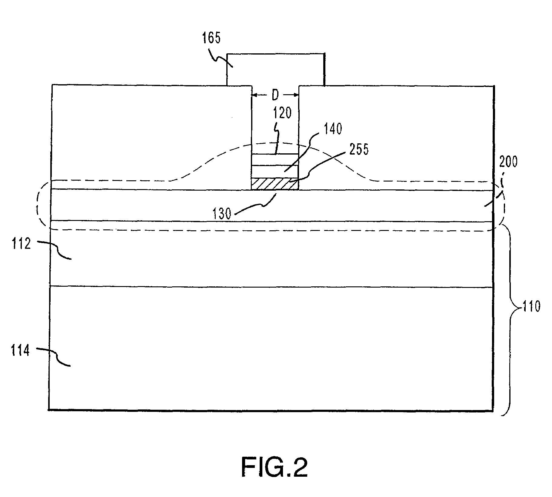
Figure 3
Abstract
Description
CROSS-REFERENCE TO RELATED APPLICATIONS
[0001] This application is a continuation of U.S. application Ser. No. 11 / 276,097 entitled “MICROELECTRONIC PROGRAMMABLE DEVICE AND METHODS OF FORMING AND PROGRAMMING THE SAME” filed on Feb. 14, 2006. The '097 application is a continuation of U.S. application Ser. No. 10 / 452,041 entitled “MICROELECTRONIC PROGRAMMABLE DEVICE AND METHODS OF FORMING AND PROGRAMMING THE SAME,” filed on May 30, 2003 and which issued as U.S. Pat. No. 6,998,312 on Feb. 14, 2006. The '041 application is a divisional of U.S. application Ser. No. 09 / 951,882, entitled “MICROELECTRONIC PROGRAMMABLE DEVICE AND METHODS OF FORMING AND PROGRAMMING THE SAME,” filed on Sep. 10, 2001 and which issued as U.S. Pat. No. 6,635,914 on Oct. 21, 2003. The '882 is a Continuation-in-Part of U.S. patent application Ser. No. 09 / 502,915, entitled “PROGRAMMABLE MICROELECTRONIC DEVICES AND METHODS OF FORMING AND PROGRAMMING SAME,” filed Feb. 11, 2000 which issued as U.S. Pat. No. 6,487,106 on N...
Examples
Embodiment Construction
[0036]The present invention generally relates to microelectronic devices. More particularly, the invention relates to programmable structures or devices suitable for various integrated circuit applications.
[0037]FIGS. 1 and 2 illustrate programmable microelectronic structures 100 and 200 formed on a surface of a substrate 110 in accordance with an exemplary embodiment of the present invention. Structures 100 and 200 include electrodes 120 and 130, an ion conductor 140, and optionally include buffer or barrier layers 155 and / or 255.
[0038]Generally, structures 100 and 200 are configured such that when a bias greater than a threshold voltage (VT), discussed in more detail below, is applied across electrodes 120 and 130, the electrical properties of structure 100 change. For example, in accordance with one embodiment of the invention, as a voltage V≧VT is applied across electrodes 120 and 130, conductive ions within ion conductor 140 begin to migrate and form an electrodeposit (e.g., el...