
Device and method for detecting small quantities of light, comprising an electronic image converter embodied in semiconductor technology
Patent Information
- Authority / Receiving Office
- US · United States
- Current Assignee / Owner
- Publication Date
- 2014-02-11
Smart Images
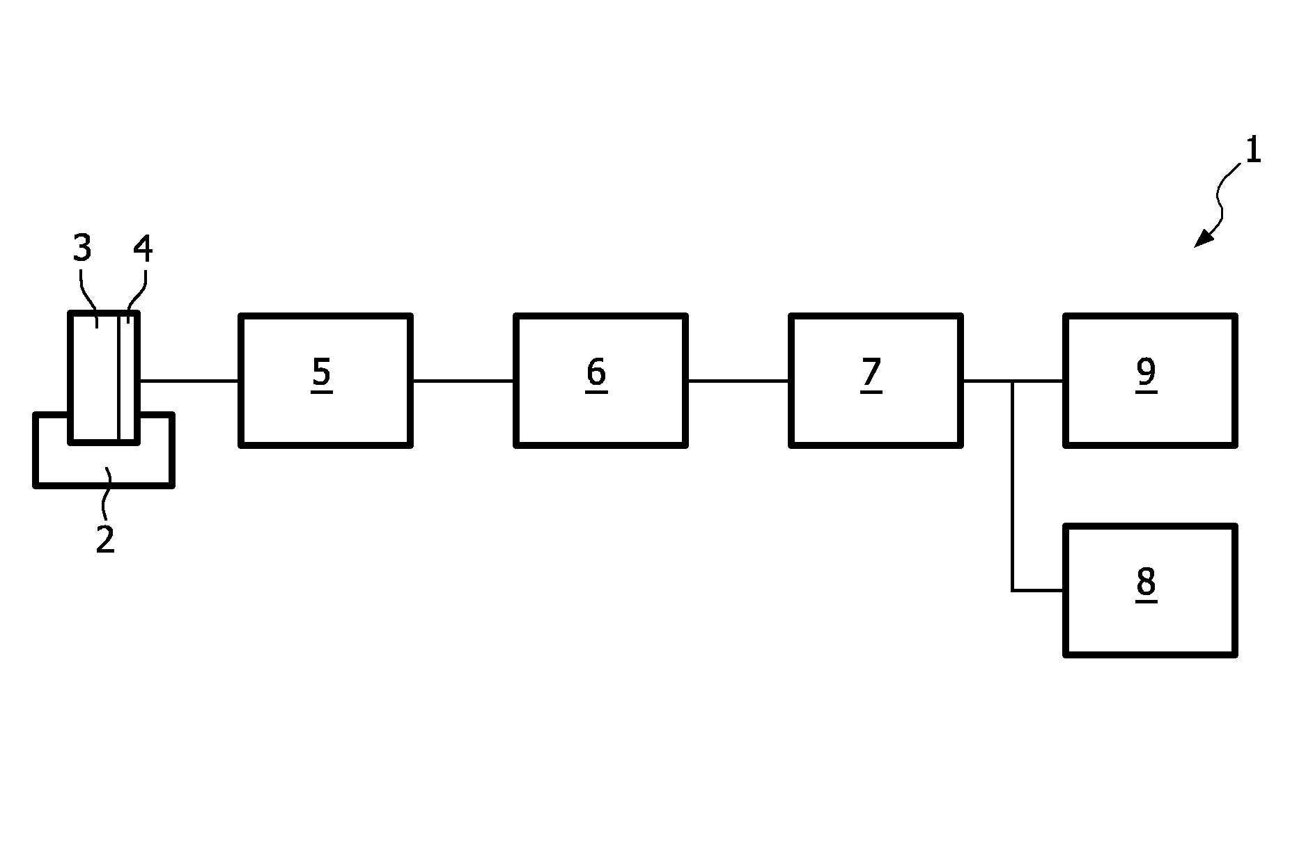
Figure 1 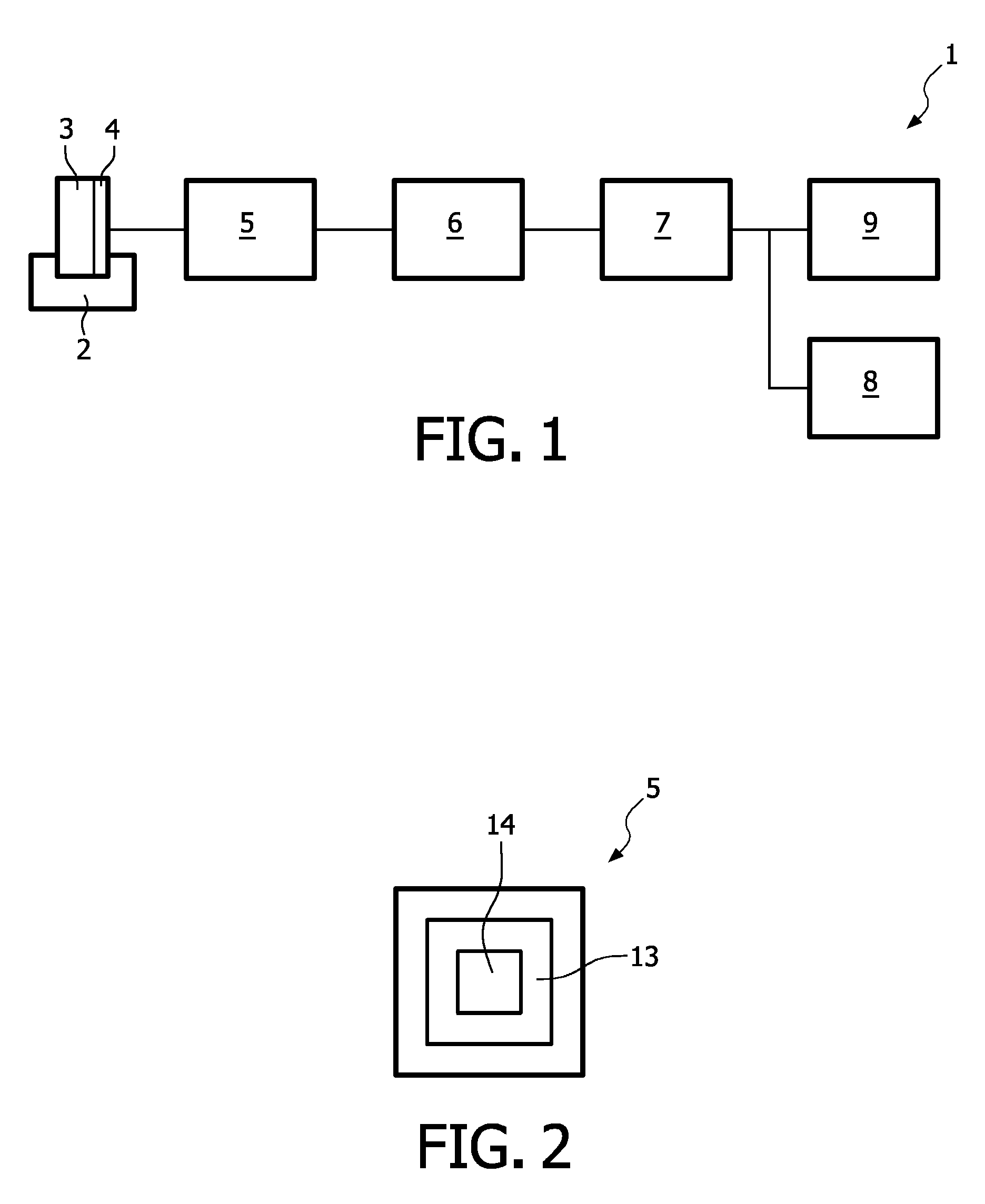
Figure 2 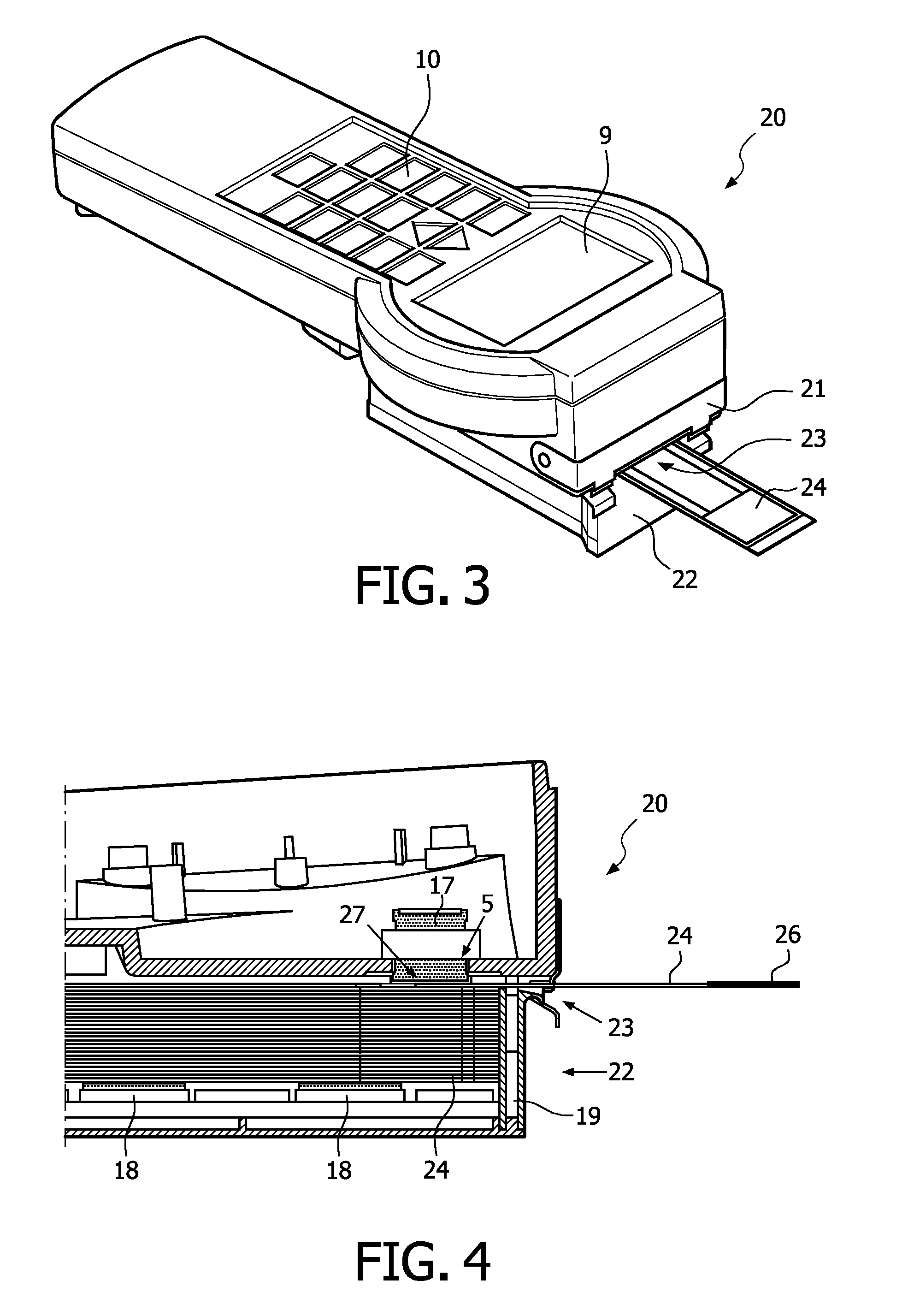
Figure 3
Abstract
Description
BACKGROUND OF THE INVENTION
[0001] 1) Field of the Invention
[0002] The invention relates to a device for detecting small quantities of light, comprising optical detection means for detecting the photons representing the small quantities of light and an electronic circuit connected to the optical detection means for reading the optical detection means and for generating a signal representing the number of photons received by the optical detection means.
[0003] 2) Description of the Related Art
[0004] Such devices are generally known. Such prior art detection devices make use of, among other parts, a photon multiplier tube, an expensive, heavy and fragile apparatus which requires a high supply voltage and which is therefore less suitable for use in the field.
[0005] In order to obviate these drawbacks the dissertation by Khaled Salama, Stanford University, September 2005, “Cmos-luminescence detection lab-on-chip modeling, design and characterisation”, provides a device for the detection of sma...
Examples
Embodiment Construction
[0035]The block diagram of FIG. 1 shows a detection device according to the present invention, designated as a whole with 1, which is suitable for functioning as detector for small quantities of light. This detection device 1 shows a positioning element 2 for positioning a carrier 3 on which a sample 4 is arranged. When necessary, a reagent can also be arranged on carrier 3 for the purpose, in co-action with the sample, of causing or improving the light-emitting action of sample 4.
[0036]The device also comprises guide means 5, for instance in the form of a tube, optionally in combination with a filter for guiding only those parts of the spectrum which are caused by the sample placed on the carrier. The guide means lead to CCD detector 5, which is connected to an electronic circuit 7. The CCD detector is provided here with 330,000 light-sensitive elements (pixels). It is otherwise also possible to place a CMOS detector instead of a CCD detector.
[0037]Electronic circuit 7 is connected...