Additive Manufacturing Of Organic Thermoelectric Devices
AUG 28, 202510 MIN READ
Generate Your Research Report Instantly with AI Agent
Patsnap Eureka helps you evaluate technical feasibility & market potential.
Organic Thermoelectric AM Technology Evolution and Objectives
Organic thermoelectric (TE) materials have evolved significantly over the past decades, transitioning from laboratory curiosities to viable alternatives to traditional inorganic thermoelectrics. The journey began in the 1970s with the discovery of conductive polymers, but meaningful thermoelectric applications only emerged in the early 2000s when researchers demonstrated that organic semiconductors could exhibit appreciable Seebeck coefficients while maintaining reasonable electrical conductivity.
The technology evolution accelerated around 2010 when poly(3,4-ethylenedioxythiophene) polystyrene sulfonate (PEDOT:PSS) emerged as a promising organic thermoelectric material, achieving power factors approaching 100 μW/mK². This milestone represented a critical turning point, as it demonstrated that organic materials could potentially compete with traditional inorganic thermoelectrics in specific applications where flexibility, lightweight properties, and low-cost manufacturing were prioritized over maximum efficiency.
Additive manufacturing (AM) techniques for organic thermoelectrics began developing in parallel around 2015, initially through rudimentary screen printing and inkjet printing methods. These early approaches suffered from limited resolution and poor control over material properties. The field has since progressed to incorporate more sophisticated techniques including aerosol jet printing, direct ink writing, and selective laser sintering, each offering unique advantages for fabricating organic thermoelectric devices.
A significant technological breakthrough occurred in 2018-2020 with the development of specialized inks and pastes formulated specifically for AM of organic thermoelectric materials. These formulations addressed critical challenges including viscosity control, particle dispersion, and post-deposition electrical performance. Concurrent advances in multi-material printing enabled the fabrication of complete thermoelectric modules in single manufacturing processes.
The primary objectives driving this technological evolution include achieving higher ZT values (thermoelectric figure of merit) in printable organic materials, developing manufacturing techniques compatible with large-scale production, and creating design methodologies that leverage AM's unique capabilities to produce novel device architectures impossible with traditional manufacturing.
Current research aims to push organic thermoelectric AM technology toward commercially viable applications by focusing on several key objectives: increasing the power factor of printable organic materials to exceed 500 μW/mK², developing printing techniques that ensure consistent material properties across large areas, creating multi-material printing processes that can seamlessly integrate conductors, semiconductors, and insulators, and establishing design rules that optimize geometric configurations for maximum power output from minimal material input.
Market Analysis for Printed Organic Thermoelectric Applications
The global market for printed organic thermoelectric applications is experiencing significant growth, driven by increasing demand for sustainable energy solutions and the advancement of flexible electronics. Current market valuations indicate that the organic thermoelectric materials market reached approximately 57 million USD in 2022, with projections suggesting a compound annual growth rate (CAGR) of 14.8% through 2030. This growth trajectory is substantially higher than traditional inorganic thermoelectric materials, reflecting the unique advantages and expanding application potential of organic alternatives.
The market segmentation for printed organic thermoelectric devices spans several key sectors. Consumer electronics represents the largest current market share, where these devices can power wearable technology, IoT sensors, and small portable devices. The healthcare sector is emerging as a rapidly growing segment, with applications in medical wearables and implantable devices that can harvest body heat to power monitoring systems. Additionally, the automotive industry is exploring integration of organic thermoelectric materials in vehicle climate control systems and for recovering waste heat from engines.
Geographically, North America and Europe currently lead in research and commercial development of organic thermoelectric technologies, accounting for approximately 65% of the global market. However, Asia-Pacific regions, particularly Japan, South Korea, and China, are demonstrating the fastest growth rates, supported by substantial investments in advanced manufacturing capabilities and favorable government policies promoting green technologies.
Key market drivers include the increasing focus on energy harvesting from waste heat sources, growing demand for self-powered sensors in IoT applications, and the push toward flexible and wearable electronics. The ability of additive manufacturing to enable customized, small-batch production of organic thermoelectric devices is particularly valuable for emerging applications where traditional manufacturing approaches are cost-prohibitive.
Market challenges remain significant, including the relatively lower efficiency of organic thermoelectric materials compared to inorganic alternatives, scalability issues in manufacturing processes, and the need for standardization across the industry. Price sensitivity is also a factor, with current production costs limiting mass-market adoption despite the technological advantages.
Industry analysts predict that as manufacturing techniques improve and material performance increases, the market for printed organic thermoelectric devices will expand into new application areas, including building energy management, military equipment, and space technology. The convergence of additive manufacturing capabilities with advances in organic semiconductor materials is expected to create new market opportunities worth over 500 million USD by 2035.
Current Challenges in Organic TE Material Additive Manufacturing
Despite significant advancements in organic thermoelectric (TE) materials, their integration into additive manufacturing processes faces several critical challenges. The primary obstacle remains the inherent trade-off between electrical conductivity and thermal conductivity in organic materials. While high electrical conductivity is desirable for efficient charge transport, the accompanying increase in thermal conductivity reduces the temperature gradient necessary for the Seebeck effect, ultimately limiting the ZT value (figure of merit) of the device.
Material stability presents another significant hurdle. Organic TE materials often degrade when exposed to oxygen, moisture, or elevated temperatures during the printing process. This degradation manifests as reduced electrical conductivity and diminished Seebeck coefficient over time, severely compromising long-term device performance and reliability in real-world applications.
The viscosity and rheological properties of organic TE materials frequently prove incompatible with existing additive manufacturing techniques. Materials that are too viscous may clog nozzles, while those with low viscosity might spread uncontrollably, resulting in poor dimensional accuracy and structural integrity. This incompatibility necessitates extensive formulation adjustments that can adversely affect the thermoelectric properties.
Interface engineering between different printed layers remains problematic. Poor adhesion between layers and the formation of interfacial barriers significantly increase contact resistance, reducing overall device efficiency. Additionally, achieving consistent doping levels throughout the printed structure is challenging, leading to performance variations within a single device.
Resolution limitations of current printing technologies restrict the fabrication of micro-scale thermoelectric devices. Most commercially available 3D printers cannot achieve the fine resolution required for optimized TE devices, particularly when attempting to create the dense arrays of p-n junctions necessary for efficient power generation.
Post-processing requirements further complicate manufacturing. Many printed organic TE materials require thermal annealing or solvent treatment to achieve optimal performance, adding complexity to the production process and potentially limiting scalability. These treatments must be carefully controlled to avoid damaging the organic components.
The lack of standardized characterization methods for additively manufactured organic TE devices impedes progress in the field. Without reliable testing protocols, comparing results across different research groups becomes difficult, slowing the pace of innovation and commercial adoption.
Finally, cost considerations remain significant. While organic materials offer potential cost advantages over inorganic alternatives, the specialized formulations required for additive manufacturing often involve expensive dopants and processing aids, challenging the economic viability of large-scale production.
Current Fabrication Methods for Printed Organic Thermoelectrics
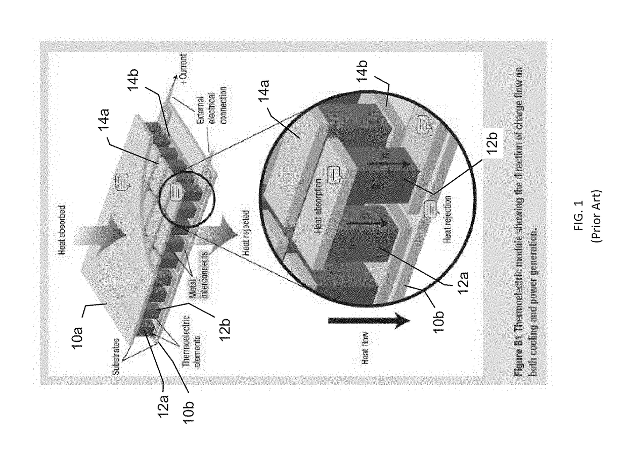
01 Organic thermoelectric materials and compositions
Various organic materials can be used in thermoelectric devices to convert heat into electricity. These materials include conducting polymers, organic semiconductors, and organic-inorganic hybrid compositions that exhibit thermoelectric properties. The selection of appropriate organic materials with high electrical conductivity and low thermal conductivity is crucial for achieving efficient thermoelectric conversion. These materials can be engineered at the molecular level to optimize their thermoelectric figure of merit (ZT).- Organic materials for thermoelectric devices: Various organic materials can be used in thermoelectric devices to convert heat into electricity. These materials include conducting polymers, organic semiconductors, and carbon-based materials that offer advantages such as flexibility, low thermal conductivity, and solution processability. The incorporation of these organic materials can enhance the thermoelectric performance through improved electrical conductivity while maintaining low thermal conductivity, which is crucial for efficient energy conversion.
- Device structure and fabrication methods: The structure and fabrication methods of organic thermoelectric devices significantly impact their performance. Various approaches include thin-film deposition, printing techniques, and layer-by-layer assembly to create optimized device architectures. These methods focus on creating efficient interfaces between different materials, controlling film thickness, and ensuring uniform material distribution to maximize the Seebeck coefficient and power factor of the devices.
- Doping strategies for enhanced performance: Doping is a critical strategy to enhance the performance of organic thermoelectric materials. By introducing dopants into organic semiconductors or polymers, the electrical conductivity can be significantly improved while maintaining relatively low thermal conductivity. Various dopants, including small molecules, metal salts, and other chemical compounds, can be used to optimize the carrier concentration and mobility in organic thermoelectric materials, leading to improved power factors and ZT values.
- Hybrid organic-inorganic thermoelectric systems: Hybrid systems combining organic materials with inorganic components can achieve enhanced thermoelectric performance. These composites leverage the advantages of both material types: the flexibility and low thermal conductivity of organic materials with the high electrical conductivity and Seebeck coefficient of inorganic materials. Nanostructuring approaches, such as incorporating inorganic nanoparticles into organic matrices, can create interfaces that scatter phonons while allowing electron transport, thereby improving the overall thermoelectric figure of merit.
- Flexible and wearable thermoelectric applications: Organic thermoelectric materials enable the development of flexible and wearable energy harvesting devices. These applications leverage the inherent mechanical flexibility of organic materials to create conformable devices that can harvest body heat or ambient thermal energy. The development focuses on creating lightweight, stretchable, and durable thermoelectric generators that can be integrated into textiles or attached directly to the skin, opening new possibilities for powering wearable electronics and IoT devices.
02 Device structure and fabrication methods
The design and fabrication of organic thermoelectric devices involve specific structural configurations to maximize energy conversion efficiency. These devices typically consist of p-type and n-type organic semiconductor layers arranged in specific patterns to create temperature differentials. Various fabrication techniques such as solution processing, printing methods, and thin-film deposition are employed to create these devices. The structural design often includes substrate selection, electrode configuration, and encapsulation methods to enhance device performance and durability.Expand Specific Solutions03 Performance enhancement techniques
Various methods can be employed to enhance the performance of organic thermoelectric devices. These include doping of organic materials to increase electrical conductivity, nanostructuring to reduce thermal conductivity, interface engineering to improve charge transport, and creating composite materials that combine the advantages of different components. Additionally, optimization of the Seebeck coefficient through molecular design and the development of flexible thermoelectric modules can significantly improve the overall efficiency and applicability of these devices.Expand Specific Solutions04 Applications and integration systems
Organic thermoelectric devices find applications in various fields including wearable electronics, waste heat recovery systems, self-powered sensors, and portable power sources. These devices can be integrated into clothing, industrial equipment, or electronic devices to harvest waste heat and convert it into usable electricity. The flexibility, lightweight nature, and potential low cost of organic thermoelectric materials make them particularly suitable for applications where conventional inorganic thermoelectric materials are impractical. Integration systems often include power management circuits and energy storage components.Expand Specific Solutions05 Testing and characterization methods
Specific methods and equipment are used to test and characterize organic thermoelectric devices. These include measurement of the Seebeck coefficient, electrical conductivity, thermal conductivity, and overall figure of merit (ZT). Advanced analytical techniques such as scanning electron microscopy, X-ray diffraction, and spectroscopic methods are employed to understand the structure-property relationships in these materials. Additionally, specialized testing setups are developed to evaluate the performance of these devices under various temperature gradients and operating conditions to determine their efficiency and stability.Expand Specific Solutions
Leading Organizations in Organic TE Additive Manufacturing
The additive manufacturing of organic thermoelectric devices market is currently in its early growth phase, characterized by intensive R&D activities and emerging commercial applications. The global market size is projected to expand significantly as energy harvesting technologies gain traction, with estimates suggesting a compound annual growth rate exceeding 15% through 2030. Technologically, the field shows varying maturity levels across different companies. Industry leaders like Merck Patent GmbH and ROHM Co. have established advanced capabilities in organic materials synthesis and device fabrication, while research institutions such as CSEM and Industrial Technology Research Institute are driving fundamental innovations. Companies including BOE Technology and Semiconductor Energy Laboratory are focusing on integration with display technologies, while DuPont and 3M are leveraging their materials expertise to develop scalable manufacturing processes. Academic-industrial partnerships are accelerating commercialization pathways in this rapidly evolving sector.
Merck Patent GmbH
Technical Solution: Merck Patent GmbH has developed a comprehensive approach to additive manufacturing of organic thermoelectric devices using specialized printing techniques. Their technology involves the formulation of printable organic semiconductor inks with optimized thermoelectric properties, particularly PEDOT:PSS (poly(3,4-ethylenedioxythiophene) polystyrene sulfonate) compounds modified with specific additives to enhance the Seebeck coefficient and electrical conductivity. The company employs multi-layer printing processes that allow precise deposition of n-type and p-type organic semiconductors to create efficient thermoelectric couples. Their manufacturing process incorporates post-deposition treatments such as controlled annealing steps to optimize the morphology and crystallinity of the printed materials, resulting in ZT values approaching 0.2-0.3 at room temperature. Merck has also developed specialized encapsulation techniques to protect the organic materials from environmental degradation, extending device lifetime significantly compared to unprotected organic thermoelectrics.
Strengths: Superior material formulation expertise with proprietary additives that enhance thermoelectric performance; established manufacturing infrastructure for scaling production; comprehensive intellectual property portfolio covering materials and processes. Weaknesses: Organic thermoelectric materials still exhibit lower ZT values compared to inorganic counterparts; long-term stability remains a challenge despite encapsulation advances.
Battelle Memorial Institute
Technical Solution: Battelle Memorial Institute has developed a comprehensive additive manufacturing platform for organic thermoelectric devices focused on scalability and industrial applications. Their approach utilizes a combination of screen printing and aerosol deposition techniques optimized for large-area fabrication of thermoelectric modules. Battelle's technology incorporates specially formulated organic semiconductor composites that combine conjugated polymers with carefully selected nanofillers to enhance electrical properties while maintaining solution processability. Their manufacturing process features multi-stage printing with intermediate curing steps that optimize layer interfaces and reduce defects. Battelle has pioneered the development of gradient-doped organic thermoelectric materials that can be printed with spatially varying carrier concentrations to optimize performance across temperature gradients. Their system includes automated quality control using electrical impedance spectroscopy to identify defects in real-time during manufacturing. Battelle has demonstrated printed organic thermoelectric modules capable of generating power densities of up to 10 μW/cm² at temperature differences of 30°C, with particular focus on waste heat recovery applications in industrial settings where temperature differences are modest but heat sources are abundant.
Strengths: Strong focus on practical applications and scalable manufacturing processes; robust quality control systems integrated into the production workflow; demonstrated performance in industrially relevant conditions. Weaknesses: Technology optimized for moderate to large-scale applications rather than miniaturized devices; performance still limited compared to traditional inorganic thermoelectric materials in high-temperature applications.
Key Patents and Breakthroughs in Organic TE Material Printing
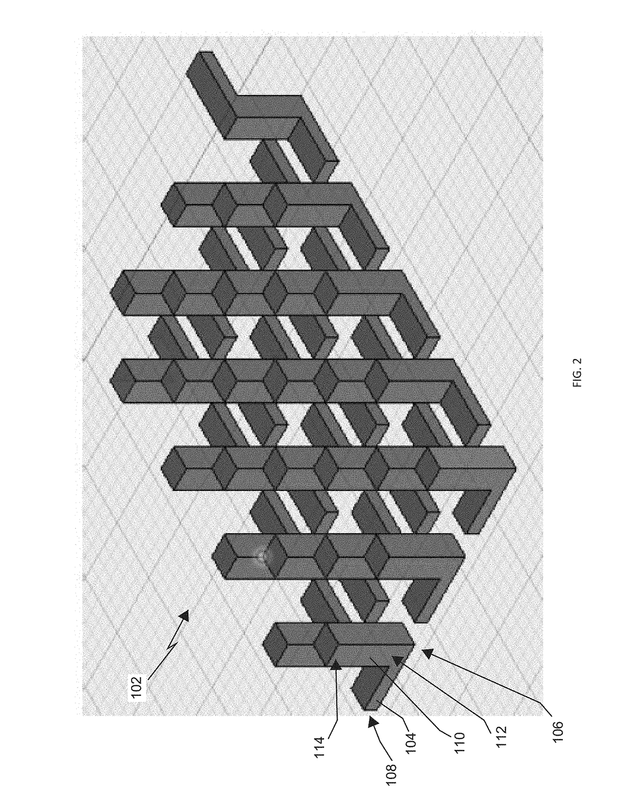
Thermoelectric Devices
PatentActiveUS20180159016A1
Innovation
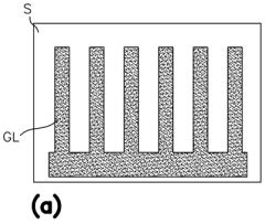
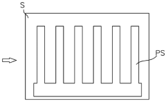
- Redesigning the thermoelectric generator to reduce distinct parts and materials, using 3-D printing to fabricate identical p-type and n-type legs and interconnects from the same conductive material, and allowing for the use of various additive manufacturing methods to simplify the assembly process and improve electrical conductivity.
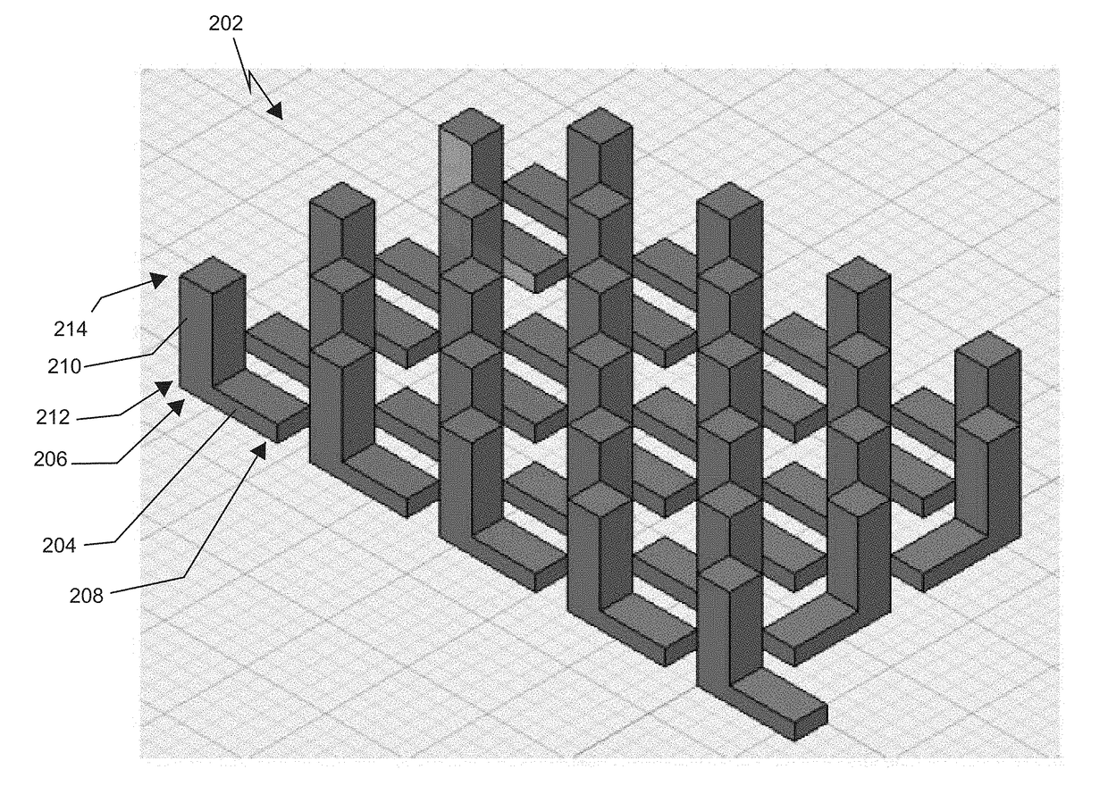
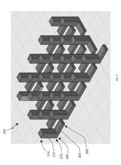
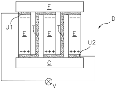
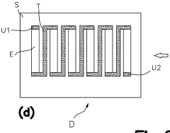
Organic thermoelectric device, thermoelectric system, method for manufacturing the device, cladding for enclosure, enclosure and solar thermal hybrid syste.
PatentActiveES2549828A1
Innovation
- A thermoelectric device with elongated, coplanar organic semiconductor polymer elements arranged on a substrate, where the hot and cold parts are separated by significant distances, eliminating the need for heat dissipation from the cold part, and using a manufacturing method that synthesizes all elements simultaneously, reducing complexity and cost.
Sustainability and Life Cycle Assessment of Printed TE Devices
The sustainability aspects of printed organic thermoelectric (TE) devices represent a critical dimension in evaluating their viability for widespread adoption. Compared to conventional inorganic TE materials which often contain rare, toxic elements like tellurium and bismuth, organic TE materials typically utilize more abundant carbon-based compounds, significantly reducing resource depletion concerns. This advantage becomes particularly pronounced when considering the global scaling potential of these technologies for energy harvesting applications.
Life cycle assessment (LCA) studies of printed organic TE devices reveal substantial environmental benefits throughout their production chain. The additive manufacturing processes employed for these devices consume significantly less material than traditional subtractive manufacturing methods, with material utilization rates often exceeding 90% compared to 40-60% in conventional approaches. Additionally, the energy requirements for processing organic materials are markedly lower, typically requiring temperatures below 200°C versus the 400-700°C needed for inorganic counterparts.
The environmental footprint of printed organic TE devices is further minimized through the elimination of harsh chemical etching processes commonly used in silicon-based electronics manufacturing. Solution-based printing techniques utilize primarily benign solvents that can be recovered and reused, reducing both waste generation and environmental contamination risks. Recent innovations in water-based and bio-derived solvent systems have further enhanced the ecological profile of these manufacturing processes.
End-of-life considerations also favor printed organic TE devices. While conventional TE modules often require specialized recycling processes to recover valuable but toxic elements, organic TE materials present fewer hazardous waste challenges. Emerging research indicates potential biodegradability pathways for certain organic semiconductors, though this remains an active area requiring further development to achieve truly circular material flows.
Energy payback time (EPBT) analyses suggest that printed organic TE devices can recover their embodied energy within 1-3 years of operation in waste heat recovery applications, compared to 3-7 years for conventional inorganic systems. This favorable EPBT is primarily attributed to the reduced energy intensity of manufacturing processes and the absence of energy-intensive purification steps required for inorganic semiconductors.
Despite these advantages, challenges remain in optimizing the operational lifespan of organic TE devices, which currently falls short of inorganic alternatives. Addressing stability and degradation mechanisms represents a critical sustainability challenge, as premature replacement negates many of the initial environmental benefits. Encapsulation technologies and molecular design strategies focused on enhancing long-term stability are therefore essential components of the sustainability equation for these emerging technologies.
Scalability and Commercialization Pathways
The scalability of additive manufacturing for organic thermoelectric devices represents a critical pathway from laboratory innovation to commercial viability. Current manufacturing processes demonstrate promising small-scale production capabilities but face significant challenges when transitioning to industrial-scale operations. The primary bottleneck lies in maintaining consistent material properties and device performance while increasing production volume, particularly for solution-processed organic thermoelectric materials that are sensitive to processing conditions.
Several technological approaches are emerging to address these scalability challenges. Roll-to-roll printing technologies offer perhaps the most promising route to mass production, enabling continuous fabrication of flexible organic thermoelectric devices on large substrate areas. Recent advancements in specialized printing heads and ink formulations have improved deposition uniformity across larger areas, reducing performance variations that previously plagued scaled production.
Material supply chains present another critical consideration for commercialization. The specialized organic semiconductors and dopants required for high-performance thermoelectric devices currently remain expensive and limited in availability. Strategic partnerships between material suppliers and device manufacturers will be essential to ensure consistent quality and reduce costs through economies of scale.
Economic viability analysis indicates that organic thermoelectric devices must achieve a manufacturing cost below $10/W to compete effectively in waste heat recovery markets. Current laboratory-scale production costs range from $50-100/W, highlighting the need for significant process optimization. The learning curve model suggests that a 20-30% cost reduction could be achieved with each doubling of production volume, potentially reaching competitive price points within 5-7 years of scaled manufacturing.
Market entry strategies for organic thermoelectric technologies will likely follow a staged approach. Initial commercialization should target niche applications where the unique properties of organic materials—flexibility, lightweight, and non-toxicity—provide distinct advantages over inorganic alternatives. Wearable electronics, IoT sensors, and specialized medical devices represent promising early markets with less price sensitivity and higher tolerance for current performance limitations.
Long-term commercial success will depend on establishing standardized testing protocols and certification processes that build market confidence in organic thermoelectric technology. Additionally, developing modular manufacturing systems that can be scaled incrementally will allow companies to expand production capacity in response to market demand while minimizing capital risk during the critical early commercialization phase.
Unlock deeper insights with Patsnap Eureka Quick Research — get a full tech report to explore trends and direct your research. Try now!
Generate Your Research Report Instantly with AI Agent
Supercharge your innovation with Patsnap Eureka AI Agent Platform!