

Nanoscale Morphology Control For Enhanced TE Performance
AUG 28, 20259 MIN READ
Generate Your Research Report Instantly with AI Agent
Patsnap Eureka helps you evaluate technical feasibility & market potential.
Nanoscale TE Technology Background and Objectives
Thermoelectric (TE) technology has evolved significantly over the past decades, transitioning from theoretical concepts to practical applications across various industries. The fundamental principle of thermoelectric effects, discovered in the early 19th century through the Seebeck, Peltier, and Thomson effects, has laid the groundwork for modern TE devices that can directly convert heat into electricity and vice versa without moving parts.
The efficiency of thermoelectric materials is primarily measured by the dimensionless figure of merit ZT, which depends on the Seebeck coefficient, electrical conductivity, and thermal conductivity. Historically, bulk thermoelectric materials have been limited by the interdependence of these parameters, resulting in relatively low ZT values (typically below 1) and limiting widespread commercial adoption beyond niche applications.
Recent advancements in nanotechnology have revolutionized the field by enabling precise control over material structure at the nanoscale. This paradigm shift has opened new pathways to decouple the traditionally interdependent thermoelectric parameters through quantum confinement effects, energy filtering, and phonon scattering mechanisms. The ability to engineer nanoscale morphology has become a critical factor in enhancing thermoelectric performance.
The global focus on sustainable energy solutions and waste heat recovery has accelerated research in thermoelectric technologies. With approximately 60% of global energy production lost as waste heat, thermoelectric generators offer a promising approach to improve energy efficiency across industrial processes, automotive applications, and consumer electronics. This potential has attracted significant investment from both public and private sectors worldwide.
Current research objectives in nanoscale thermoelectric technology center on achieving ZT values consistently above 2 at practical operating temperatures, developing scalable and cost-effective manufacturing processes, and creating environmentally sustainable materials that reduce or eliminate rare and toxic elements. Particular emphasis is placed on understanding and controlling interfaces, grain boundaries, and defects at the nanoscale to optimize electron transport while minimizing thermal conductivity.
The convergence of advanced characterization techniques, computational modeling, and innovative synthesis methods has accelerated progress in this field. High-resolution transmission electron microscopy, scanning probe techniques, and synchrotron-based spectroscopies now allow researchers to visualize and manipulate structures at atomic scales, providing unprecedented insights into structure-property relationships in thermoelectric nanomaterials.
Looking forward, the field aims to develop "designer" thermoelectric materials with precisely engineered nanoscale features that can be tailored for specific temperature ranges and applications. The ultimate goal is to create highly efficient, durable, and cost-effective thermoelectric systems that can make meaningful contributions to global energy challenges and sustainability efforts.
Market Analysis for Thermoelectric Applications
The global thermoelectric (TE) market is experiencing significant growth, driven by increasing demand for energy efficiency solutions and waste heat recovery systems. Current market valuations place the thermoelectric materials and devices sector at approximately 600 million USD in 2023, with projections indicating growth to reach 1.2 billion USD by 2030, representing a compound annual growth rate of 10.4%.
Automotive applications currently dominate the thermoelectric market, accounting for nearly 35% of total market share. This segment utilizes thermoelectric generators (TEGs) to convert waste heat from engine exhaust into usable electricity, improving overall vehicle efficiency. Major automotive manufacturers including BMW, Ford, and Toyota have active research programs investigating advanced thermoelectric solutions.
The consumer electronics sector represents the fastest-growing application area, with an estimated growth rate of 14.2% annually. Thermoelectric cooling solutions for processors, wearable devices, and portable refrigeration units are gaining traction as manufacturers seek energy-efficient thermal management solutions. Companies like Samsung and Apple are exploring thermoelectric technologies for next-generation devices.
Industrial waste heat recovery presents perhaps the most significant long-term market opportunity. With global industrial processes wasting approximately 20-50% of consumed energy as heat, the potential for thermoelectric generation is substantial. Early adopters include steel manufacturing, chemical processing, and power generation industries, where high-temperature waste streams provide ideal conditions for thermoelectric energy harvesting.
Medical and aerospace applications represent smaller but premium market segments with higher profit margins. Thermoelectric cooling for precise temperature control in medical devices and spacecraft thermal management systems commands premium pricing due to reliability requirements and specialized performance needs.
Geographically, North America and Asia-Pacific regions lead in thermoelectric technology adoption. North America dominates in research and development activities, while Asia-Pacific, particularly China, Japan, and South Korea, leads in manufacturing capacity and implementation. Europe shows strong growth potential driven by stringent energy efficiency regulations and sustainability initiatives.
Market barriers include relatively high costs compared to conventional technologies, with current thermoelectric solutions averaging $8-15 per watt of capacity. Additionally, efficiency limitations of commercial thermoelectric materials (ZT values typically below 1.5) restrict widespread adoption in cost-sensitive applications. This highlights the critical importance of nanoscale morphology control research, as improvements in ZT values to 2.0 or higher could potentially reduce costs by 30-40%, significantly expanding addressable markets.
Current Challenges in Nanoscale Morphology Control
Despite significant advancements in thermoelectric (TE) materials, controlling nanoscale morphology remains one of the most challenging aspects in enhancing TE performance. The fundamental challenge lies in simultaneously optimizing the three interdependent transport parameters: electrical conductivity, thermal conductivity, and Seebeck coefficient. Nanoscale morphology directly influences these parameters, yet manipulating structures at this scale presents considerable technical difficulties.
Precise fabrication at the nanoscale encounters significant reproducibility issues. Current manufacturing processes struggle to consistently produce identical nanostructures with the exact dimensions and orientations required for optimal TE performance. This variability leads to inconsistent material properties and device performance, hampering commercial viability and scalability.
Interface engineering presents another major challenge. The boundaries between different phases or components in nanostructured TE materials often introduce undesirable electron scattering effects while not effectively scattering phonons as intended. Controlling these interfaces to selectively scatter phonons while maintaining electron transport remains elusive, particularly in complex composite systems where multiple interfaces exist.
Stability of nanoscale morphology under operating conditions poses a critical challenge. TE devices typically operate under significant temperature gradients and thermal cycling, which can lead to degradation of carefully engineered nanostructures through processes such as coarsening, phase segregation, or atomic diffusion. This morphological evolution during operation often results in performance deterioration over time.
Characterization limitations further complicate progress in this field. Current analytical techniques struggle to provide comprehensive three-dimensional information about nanoscale morphology in real-time during device operation. Most characterization methods offer either high spatial resolution with limited temporal resolution or vice versa, making it difficult to understand dynamic morphological changes.
The scalable synthesis of optimized nanomorphologies represents perhaps the most significant barrier to commercial implementation. Laboratory-scale techniques that produce excellent results often rely on processes that are prohibitively expensive or time-consuming for industrial production. Bridging this gap between lab-scale success and industrial viability requires developing new synthesis approaches that maintain nanoscale control while being amenable to mass production.
Additionally, theoretical models predicting the relationship between specific nanomorphologies and resulting TE properties remain incomplete. The multiphysics nature of thermoelectric phenomena, involving coupled electrical, thermal, and structural effects at the nanoscale, creates enormous computational challenges that current simulation capabilities struggle to address comprehensively.
Current Nanoscale Morphology Control Techniques
01 Novel thermoelectric materials composition
Various novel compositions have been developed to enhance thermoelectric performance. These include nanostructured materials, composite materials, and materials with specific dopants that can significantly improve the figure of merit (ZT). These novel compositions often feature reduced thermal conductivity while maintaining or improving electrical conductivity, leading to higher energy conversion efficiency. The materials are designed with optimized carrier concentration and mobility to maximize the power factor.- Novel thermoelectric materials composition: Various novel compositions have been developed to enhance thermoelectric performance. These include nanostructured materials, composite materials, and materials with specific dopants that can significantly improve the figure of merit (ZT). These compositions are designed to simultaneously increase electrical conductivity while reducing thermal conductivity, which is crucial for efficient thermoelectric energy conversion. The materials often incorporate elements like bismuth, tellurium, lead, or silicon in specific crystalline structures or alloys.
- Nanostructuring techniques for thermoelectric efficiency: Nanostructuring has emerged as a key approach to enhance thermoelectric performance by creating phonon scattering centers while maintaining electron transport. Techniques include creating nanowires, quantum dots, superlattices, and other nanostructured architectures that can effectively reduce thermal conductivity without significantly affecting electrical conductivity. These approaches often involve precise control of material dimensions at the nanoscale to optimize the power factor and thermoelectric figure of merit.
- Fabrication methods for high-performance thermoelectric devices: Advanced fabrication methods have been developed to produce high-performance thermoelectric devices. These include techniques such as spark plasma sintering, hot pressing, melt spinning, and various deposition methods that can control the microstructure and interfaces within thermoelectric materials. These processing techniques are crucial for maintaining the desired properties of thermoelectric materials while forming them into functional devices with optimal electrical contacts and thermal management.
- Flexible and wearable thermoelectric generators: Recent innovations have focused on developing flexible and wearable thermoelectric generators that can harvest body heat or ambient temperature differences. These devices utilize specially designed flexible substrates, organic thermoelectric materials, or thin-film technologies that can conform to curved surfaces while maintaining thermoelectric performance. Such flexible generators are particularly promising for powering wearable electronics, medical devices, and Internet of Things (IoT) sensors.
- Enhancement of thermoelectric figure of merit (ZT): Various strategies have been developed to enhance the thermoelectric figure of merit (ZT), which is a key indicator of thermoelectric performance. These approaches include band engineering, energy filtering, modulation doping, and creating materials with complex crystal structures. The goal is to optimize the power factor (S²σ, where S is the Seebeck coefficient and σ is electrical conductivity) while minimizing thermal conductivity. Advanced characterization techniques are also employed to understand and improve the fundamental transport properties that contribute to ZT.
02 Nanostructuring techniques for thermoelectric materials
Nanostructuring techniques are employed to enhance thermoelectric performance by introducing nanoscale features that scatter phonons without significantly affecting electron transport. These techniques include creating nanopores, nanoinclusions, quantum dots, and nanolayers. By engineering materials at the nanoscale, thermal conductivity can be reduced through increased phonon scattering at interfaces, while maintaining electrical properties, thereby improving the overall thermoelectric figure of merit.Expand Specific Solutions03 Thin film thermoelectric devices
Thin film thermoelectric technologies offer advantages in terms of material efficiency, flexibility, and integration capabilities. These films can be deposited using various techniques such as sputtering, evaporation, or solution-based methods. The performance of thin film thermoelectric materials can be enhanced through careful control of film thickness, interface engineering, and substrate selection. These devices are particularly suitable for small-scale energy harvesting and localized cooling applications.Expand Specific Solutions04 Skutterudite and half-Heusler compounds
Skutterudite and half-Heusler compounds represent important classes of thermoelectric materials with promising performance characteristics. These materials feature complex crystal structures that inherently reduce thermal conductivity while maintaining good electrical properties. Their performance can be further enhanced through filling the voids in the crystal structure with rattler atoms (in skutterudites) or through precise control of composition and doping (in half-Heuslers). These compounds offer good thermal stability and can operate efficiently at medium to high temperatures.Expand Specific Solutions05 Organic and flexible thermoelectric materials
Organic and flexible thermoelectric materials represent an emerging class of materials that offer advantages in terms of mechanical flexibility, low-temperature processing, and reduced environmental impact. These materials include conducting polymers, organic-inorganic hybrids, and carbon-based materials. While their thermoelectric performance is generally lower than inorganic counterparts, they offer unique advantages for wearable electronics, conformal energy harvesting, and large-area applications where flexibility and form factor are critical considerations.Expand Specific Solutions
Leading Players in Thermoelectric Technology
The nanoscale morphology control for enhanced thermoelectric (TE) performance market is currently in a growth phase, with increasing research focus from both academic institutions and industry players. The global thermoelectric market is projected to expand significantly due to rising demand for energy-efficient technologies. Leading research institutions like The University of Texas System, University of California, and Chinese universities (Zhejiang, Nankai, Shanghai Institute of Ceramics) are advancing fundamental science, while corporations such as Toyota, TSMC, and Honda are exploring commercial applications. The technology remains in mid-maturity stage, with significant breakthroughs in nanoscale control techniques emerging from collaborative efforts between academia and industry partners like Battelle Memorial Institute and UT-Battelle LLC, indicating a competitive landscape balanced between theoretical research and practical implementation.
The Regents of the University of California
Technical Solution: The University of California has developed a comprehensive platform for nanoscale morphology control in thermoelectric materials through their "Integrated Nanostructure Engineering" approach. Their technology leverages advanced epitaxial growth techniques combined with post-synthesis treatments to create precisely engineered nanostructures with optimized thermoelectric properties. The university's research teams have pioneered methods for controlled introduction of nanoscale defects, interfaces, and compositional modulations that effectively scatter phonons while preserving electronic transport[7]. Their approach includes the development of superlattice structures with atomically sharp interfaces that create quantum confinement effects beneficial for thermoelectric performance. UC researchers have demonstrated particular success with silicon-germanium nanocomposites and oxide-based thermoelectric systems, achieving significant ZT enhancements through careful manipulation of nanoscale features[8]. Their technology incorporates advanced thin-film deposition techniques that enable precise layer-by-layer growth of complex thermoelectric heterostructures. The university has also developed specialized in-situ characterization methods that provide real-time feedback during nanostructure formation, enabling more precise control over morphological development. Their approach combines experimental techniques with theoretical modeling to predict optimal nanoscale architectures for specific material systems and operating conditions.
Strengths: Exceptional capabilities in epitaxial growth and thin-film deposition techniques that enable precise control over nanoscale features; strong integration of advanced characterization methods with synthesis processes. Weaknesses: Some of their most effective approaches are currently limited to thin-film geometries that may not be suitable for all thermoelectric applications; certain nanoscale features require specialized deposition equipment that may limit widespread adoption.
Wuhan University of Technology
Technical Solution: Wuhan University of Technology has developed a comprehensive approach to nanoscale morphology control for enhanced thermoelectric performance centered on novel solution-based synthesis methods. Their technology employs controlled precipitation and crystallization processes to create precisely engineered nanostructures with optimized interfaces and boundaries. The university's research team has pioneered the use of hydrothermal/solvothermal synthesis techniques that enable atomic-level control over composition and structure, resulting in thermoelectric materials with significantly reduced lattice thermal conductivity[3]. Their approach includes the development of core-shell nanostructures and hierarchical architectures that create multiple phonon scattering mechanisms across different length scales. The university has demonstrated particular success with bismuth telluride-based systems, achieving ZT values approaching 2.0 through careful manipulation of grain boundaries, defect engineering, and nanoinclusions[4]. Their technology also incorporates post-synthesis treatments such as controlled annealing processes that optimize carrier concentration while preserving beneficial nanoscale features. The university has further developed in-situ characterization techniques that allow real-time monitoring of nanostructure evolution during synthesis, enabling more precise control over morphological development.
Strengths: Exceptional capabilities in solution-based synthesis methods that allow precise control over nanoscale features; strong integration of computational modeling with experimental approaches to predict optimal morphologies. Weaknesses: Some of their solution-based methods face challenges in scaling to industrial production volumes; certain nanoscale features can agglomerate or coarsen during extended operation at elevated temperatures, potentially reducing long-term performance stability.
Key Innovations in TE Material Nanostructuring
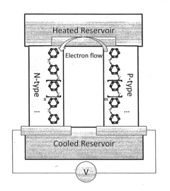
Molecular thermoelectric device
PatentWO2011100438A2
Innovation
- The development of thermoelectric devices with quantum conductors that exhibit transmission nodes or resonances due to quantum interference, specifically utilizing Single-Molecule Junctions (SMJs) with N-type and P-type organic molecules in self-assembled monolayers, enhancing thermoelectric effects through scalable order-dependent quantum responses.
Molecular thermoelectric device
PatentInactiveUS20120318317A1
Innovation
- The development of thermoelectric devices with quantum conductors that exhibit transmission nodes or resonances due to quantum interference, such as Single-Molecule Junctions (SMJs) with higher-order supernodes, enhancing the thermoelectric response by optimizing the transmission probability and interference effects.
Sustainability Aspects of TE Materials
The sustainability of thermoelectric (TE) materials represents a critical dimension in evaluating their long-term viability and environmental impact. As nanoscale morphology control emerges as a key strategy for enhancing TE performance, examining the sustainability aspects becomes increasingly important for responsible technology development.
Material abundance and resource scarcity constitute primary sustainability concerns for TE technologies. Many high-performance TE materials incorporate rare or toxic elements such as tellurium, bismuth, and lead. Nanoscale morphology control offers promising pathways to reduce reliance on these critical materials by enhancing performance efficiency through structural optimization rather than compositional adjustments, potentially enabling the use of more abundant elements while maintaining competitive performance metrics.
Energy payback time—the duration required for a TE device to generate the energy consumed during its production—significantly improves through nanoscale engineering. By enhancing conversion efficiency through controlled morphology at the nanoscale, the operational lifetime value of TE devices increases, justifying the initial energy investment in their fabrication and deployment.
Life cycle assessment (LCA) of nanoscale-engineered TE materials reveals complex sustainability profiles. While nanofabrication processes often require specialized equipment and energy-intensive conditions, the resulting performance enhancements can offset these impacts through extended operational lifetimes and improved efficiency. Comprehensive LCA studies indicate that morphology-optimized TE materials can achieve net environmental benefits when deployed in appropriate applications.
Manufacturing scalability presents both challenges and opportunities for sustainable implementation. Current precision nanofabrication techniques often involve resource-intensive processes with limited throughput. Developing scalable methods for nanoscale morphology control, such as solution-based processing and self-assembly approaches, represents a crucial frontier for improving the sustainability profile of advanced TE materials.
End-of-life management and recyclability considerations are increasingly important as TE technology deployment expands. Nanoscale engineering affects material recoverability, with some morphological features potentially complicating conventional recycling processes. Research into design-for-disassembly approaches and specialized recovery techniques for nanoscale-engineered TE materials shows promise for closing material loops and minimizing waste.
Regulatory frameworks and environmental standards are evolving to address the unique considerations of nanomaterials. Manufacturers implementing nanoscale morphology control for TE performance enhancement must navigate these emerging requirements, balancing performance optimization with compliance and environmental stewardship throughout the product lifecycle.
Scalability and Manufacturing Considerations
The transition from laboratory-scale synthesis to industrial production represents a critical challenge for nanoscale thermoelectric materials. Current laboratory methods for controlling nanoscale morphology often involve complex processes with precise parameter control that are difficult to scale. Batch-to-batch variations in nanoscale features can significantly impact thermoelectric performance, necessitating robust quality control protocols during manufacturing.
Mass production of thermoelectric materials with controlled nanoscale morphology requires adaptation of existing fabrication techniques. Solution-based processing methods show particular promise, as they can be integrated into roll-to-roll manufacturing systems. However, maintaining precise control over nanostructure formation during high-volume production remains technically challenging and cost-intensive.
Economic considerations play a crucial role in commercialization efforts. The cost-performance ratio must be optimized to compete with conventional energy technologies. Current manufacturing approaches for nanoscale thermoelectric materials typically involve expensive equipment and energy-intensive processes, resulting in prohibitively high production costs for many applications.
Environmental and safety concerns also impact manufacturing scalability. Many nanomaterial synthesis routes utilize toxic precursors or generate hazardous waste streams. Developing greener synthesis methods that maintain nanoscale morphology control while reducing environmental impact represents an important research direction for industrial implementation.
Recent advances in additive manufacturing offer new opportunities for scalable production. 3D printing technologies capable of depositing thermoelectric materials with controlled microstructures are emerging, potentially enabling customized geometries optimized for specific applications. However, achieving the necessary resolution for nanoscale features remains challenging with current printing technologies.
Standardization of characterization methods for nanoscale morphology is essential for quality assurance in manufacturing. Developing rapid, non-destructive testing protocols that can be implemented in production lines would significantly enhance scalability. Current analytical techniques often require specialized equipment and expertise not readily available in manufacturing environments.
Strategic partnerships between academic institutions and industry will be crucial for addressing these manufacturing challenges. Collaborative efforts can accelerate the development of scalable processes by combining fundamental research insights with practical engineering expertise. Such partnerships have already yielded promising results in pilot-scale production of nanostructured thermoelectric modules.
Unlock deeper insights with Patsnap Eureka Quick Research — get a full tech report to explore trends and direct your research. Try now!
Generate Your Research Report Instantly with AI Agent
Supercharge your innovation with Patsnap Eureka AI Agent Platform!