Analysis of Spray Drying Methods for Semiconductor Fabrication
SEP 25, 20259 MIN READ
Generate Your Research Report Instantly with AI Agent
Patsnap Eureka helps you evaluate technical feasibility & market potential.
Semiconductor Spray Drying Technology Evolution and Objectives
Spray drying technology in semiconductor fabrication has evolved significantly over the past several decades, transforming from a peripheral process to a critical manufacturing technique. Initially developed in the food and pharmaceutical industries, spray drying was adapted for semiconductor applications in the late 1980s when manufacturers sought more efficient methods for producing ceramic powders used in electronic components.
The evolution of semiconductor spray drying technology can be traced through distinct phases. The first phase (1980s-1990s) focused on basic adaptation of existing spray drying equipment for semiconductor materials. During this period, the primary objective was simply to achieve uniform particle size distribution for basic ceramic substrates and packaging materials.
The second phase (1990s-2000s) saw significant refinements in process control and equipment design specifically for semiconductor applications. This period coincided with the rapid miniaturization of electronic components, which demanded increasingly precise particle characteristics. Manufacturers developed specialized atomizers and chamber designs to achieve tighter control over particle morphology and composition.
The third phase (2000s-2010s) was characterized by integration of spray drying into advanced semiconductor manufacturing processes. During this period, the technology expanded beyond simple powder production to include specialized applications such as precursor preparation for thin film deposition and nanomaterial synthesis for next-generation devices.
Currently, we are in the fourth phase (2010s-present) where spray drying technology is being optimized for emerging semiconductor materials and architectures. This includes applications in wide-bandgap semiconductors, flexible electronics, and quantum computing components. The focus has shifted toward precision engineering of multi-component materials with controlled porosity, crystallinity, and surface functionality.
The primary objectives of modern semiconductor spray drying technology are multifaceted. First, achieving nanoscale precision in particle size distribution (typically targeting <5% deviation) is essential for consistent electrical and mechanical properties. Second, maintaining chemical purity at parts-per-billion levels is critical for preventing device contamination and failure. Third, enabling scalable production of advanced materials is necessary to support commercial manufacturing volumes.
Looking forward, the technology roadmap for semiconductor spray drying aims to address several key challenges. These include developing processes for novel 2D materials, enhancing energy efficiency of the drying process, and integrating real-time monitoring systems for quality control. The ultimate goal is to establish spray drying as a versatile platform technology capable of supporting the increasingly diverse material requirements of next-generation semiconductor devices.
Market Demand Analysis for Advanced Semiconductor Fabrication
The semiconductor industry is experiencing unprecedented growth, with the global market projected to reach $1 trillion by 2030. This expansion is driven by increasing demand for advanced chips in emerging technologies such as artificial intelligence, 5G networks, autonomous vehicles, and Internet of Things (IoT) devices. Within this landscape, advanced fabrication techniques like spray drying methods are becoming increasingly critical to meet the industry's evolving requirements for smaller, more efficient, and more powerful semiconductor components.
Market research indicates that the demand for spray drying technologies in semiconductor fabrication is growing at a compound annual growth rate of 7.8%, significantly outpacing traditional manufacturing methods. This growth is primarily attributed to spray drying's ability to produce uniform, high-purity powders with precise particle size distribution, which is essential for next-generation semiconductor materials.
The Asia-Pacific region, particularly Taiwan, South Korea, and China, represents the largest market for advanced semiconductor fabrication technologies, accounting for approximately 65% of global demand. This regional dominance is expected to continue as these countries invest heavily in expanding their semiconductor manufacturing capabilities to reduce dependence on foreign technologies and secure their position in the global supply chain.
Consumer electronics remains the largest end-use segment for semiconductors produced using advanced fabrication methods, representing 42% of the market. However, automotive applications are showing the fastest growth rate at 12.3% annually, driven by the increasing semiconductor content in modern vehicles, particularly electric and autonomous models.
Industry surveys reveal that manufacturers are willing to pay premium prices for fabrication technologies that can deliver higher yields, reduced material waste, and enhanced product performance. Spray drying methods, which can achieve these objectives, are therefore commanding significant market interest despite their higher initial implementation costs.
Environmental regulations and sustainability concerns are also shaping market demand. Spray drying methods that reduce water consumption, energy usage, and hazardous waste generation are gaining preference among manufacturers seeking to comply with stricter environmental standards and achieve corporate sustainability goals.
The COVID-19 pandemic and subsequent global chip shortage have accelerated demand for localized, resilient semiconductor supply chains, creating new market opportunities for advanced fabrication technologies that can be deployed in diverse geographic locations with minimal infrastructure requirements. Spray drying methods, with their relatively compact footprint and adaptability, are well-positioned to benefit from this trend.
Current Spray Drying Techniques and Technical Barriers
Spray drying technology in semiconductor fabrication has evolved significantly over the past decade, with several distinct techniques now employed across the industry. Conventional spray drying methods utilize atomization through pressure nozzles, two-fluid nozzles, or rotary atomizers to create fine droplets of semiconductor material solutions or suspensions. These systems typically operate at temperatures between 150-300°C, with residence times of milliseconds to seconds, allowing for rapid evaporation while maintaining material integrity.
Advanced spray drying techniques have emerged specifically for semiconductor applications, including ultrasonic spray drying which produces exceptionally uniform droplets in the 1-10 μm range—critical for high-precision semiconductor materials. Pulse combustion spray drying, offering enhanced energy efficiency and tighter particle size distribution, has gained traction for specialized semiconductor powder production. Electrospray drying, utilizing electrostatic forces for atomization, enables production of nanoparticles with precisely controlled morphology.
Despite these advancements, significant technical barriers persist. Temperature control remains challenging, as many semiconductor materials are thermally sensitive, with degradation thresholds sometimes within 5-10°C of optimal processing temperatures. Even minor temperature fluctuations can lead to crystal structure alterations, affecting electrical properties and device performance. This necessitates sophisticated thermal management systems that add complexity and cost.
Particle size consistency presents another major hurdle. While current technologies can achieve coefficient of variation values around 15-20%, next-generation semiconductor applications demand uniformity below 10%. The industry struggles with scaling production while maintaining this precision, particularly for materials requiring sub-micron particle sizes. Agglomeration during the drying process further complicates size control efforts.
Contamination control represents perhaps the most stringent requirement, as even parts-per-billion impurities can compromise semiconductor performance. Current spray drying systems struggle to maintain ultra-high purity environments throughout the process chain. Material contact surfaces, air handling systems, and process controls must all meet cleanroom standards that exceed those of pharmaceutical applications by orders of magnitude.
Scalability challenges are evident when transitioning from laboratory to production environments. Maintaining consistent quality while increasing throughput often requires complete system redesigns rather than simple scale-up. The complex interplay between process parameters becomes increasingly difficult to manage at larger scales, with small variations amplifying through the system.
Energy efficiency remains suboptimal, with current spray drying systems for semiconductor materials typically operating at 30-40% thermal efficiency. This not only increases production costs but also creates thermal management challenges in cleanroom environments where precise temperature and humidity control is essential.
Mainstream Spray Drying Solutions for Semiconductor Manufacturing
01 Spray drying equipment and apparatus design
Various designs of spray drying equipment and apparatus have been developed to improve efficiency and product quality. These designs include specialized chambers, nozzles, and atomizers that control particle size and distribution. Advanced systems incorporate features for temperature control, airflow management, and collection of dried particles, enhancing the overall spray drying process and resulting in more consistent product characteristics.- Spray drying equipment and apparatus design: Various designs and configurations of spray drying equipment have been developed to improve efficiency and product quality. These include specialized chambers, nozzle arrangements, and integrated systems that optimize the drying process. Advanced designs incorporate features for controlling air flow patterns, temperature gradients, and particle formation dynamics, resulting in better control over the final product characteristics.
- Process parameters optimization for spray drying: Optimization of process parameters is crucial for effective spray drying. Key parameters include inlet and outlet temperatures, feed rate, atomization pressure, and air flow rates. By carefully controlling these variables, manufacturers can achieve desired particle size distribution, moisture content, and powder properties. Advanced monitoring and control systems enable real-time adjustments to maintain optimal conditions throughout the drying process.
- Formulation techniques for spray-dried products: Specialized formulation techniques have been developed to enhance the properties of spray-dried products. These include the addition of carriers, stabilizers, and other excipients that improve flowability, stability, and dissolution characteristics. Formulation strategies can be tailored to specific applications, such as pharmaceuticals, food products, or industrial materials, resulting in powders with enhanced functionality and performance.
- Novel applications of spray drying technology: Spray drying technology has expanded beyond traditional applications to include novel uses in various industries. These include the production of advanced materials, encapsulation of sensitive compounds, and development of specialized delivery systems. The versatility of spray drying allows for the creation of unique particle structures with controlled release properties, enhanced bioavailability, or specific functional characteristics tailored to diverse applications.
- Sustainable and energy-efficient spray drying methods: Innovations in spray drying focus on improving energy efficiency and sustainability. These include heat recovery systems, alternative energy sources, and process intensification techniques that reduce energy consumption and environmental impact. Advanced designs incorporate recirculation of drying gases, improved insulation, and optimized atomization methods to minimize resource use while maintaining product quality and production rates.
02 Process parameters optimization for spray drying
Optimization of process parameters is crucial for effective spray drying operations. Key parameters include inlet and outlet temperatures, feed rate, atomization pressure, and air flow rate. By carefully controlling these variables, manufacturers can achieve desired particle characteristics, moisture content, and product stability. Advanced monitoring systems allow for real-time adjustments to maintain optimal conditions throughout the drying process.Expand Specific Solutions03 Formulation techniques for spray-dried products
Specific formulation techniques have been developed to enhance the properties of spray-dried products. These include the addition of carriers, stabilizers, and other excipients that improve flowability, stability, and dissolution characteristics. Formulation strategies may involve pre-treatment of feed solutions, adjustment of solid content, pH modification, or incorporation of functional additives to achieve desired product attributes after spray drying.Expand Specific Solutions04 Specialized spray drying for sensitive materials
Specialized spray drying methods have been developed for heat-sensitive materials such as proteins, enzymes, probiotics, and certain pharmaceuticals. These methods employ lower temperatures, protective excipients, or modified drying environments to preserve biological activity and structural integrity. Techniques may include co-current flow designs, two-fluid nozzles, or the use of inert gases to create oxygen-depleted environments during the drying process.Expand Specific Solutions05 Industrial applications of spray drying technology
Spray drying technology has been adapted for various industrial applications across multiple sectors. In the food industry, it's used for producing powdered milk, instant coffee, and flavor encapsulation. Pharmaceutical applications include the production of inhalable powders and improved bioavailability formulations. Other industries utilize spray drying for ceramic powder production, catalyst preparation, and specialty chemical manufacturing, each with specific modifications to the basic spray drying process.Expand Specific Solutions
Key Industry Players and Competitive Landscape
The semiconductor spray drying technology market is in a growth phase, characterized by increasing demand for advanced fabrication methods that enhance efficiency and precision. The global market size is expanding rapidly, driven by the semiconductor industry's continuous evolution towards smaller, more complex chip designs. Technologically, spray drying methods are maturing, with key players like TSMC, Samsung Electronics, and Lam Research leading innovation through substantial R&D investments. Companies such as Tokyo Electron, NAURA Microelectronics, and Renesas Electronics are developing specialized spray drying solutions that address critical challenges in semiconductor manufacturing, including particle contamination reduction and uniform coating deposition. The competitive landscape is intensifying as traditional semiconductor equipment manufacturers compete with specialized chemical companies like Sumitomo Bakelite and Central Glass to develop integrated spray drying systems that meet increasingly stringent fabrication requirements.
Samsung Electronics Co., Ltd.
Technical Solution: Samsung Electronics has developed a proprietary spray drying technology for semiconductor materials that focuses on scalability and precision for high-volume manufacturing environments. Their system employs a hybrid atomization approach combining pressure and ultrasonic mechanisms to achieve optimal droplet size control across varying production volumes. Samsung's technology features a vertical counter-current drying chamber design that maximizes residence time while minimizing equipment footprint, crucial for space-constrained semiconductor fabrication facilities[3]. The system incorporates advanced computational modeling to predict and control particle formation dynamics, allowing for precise engineering of powder characteristics such as flowability, compressibility, and sinterability. Samsung has particularly focused on optimizing their spray drying process for dielectric and semiconductor packaging materials, achieving particle size uniformity with standard deviations below 2.5μm and moisture content consistently below 0.5%[6]. Their technology also includes an integrated reclamation system that recovers and purifies solvents, reducing environmental impact and operating costs.
Strengths: Highly scalable from R&D to mass production without significant parameter adjustments; excellent energy efficiency with heat recovery systems reducing energy consumption by approximately 30%; superior particle morphology control. Weaknesses: Higher initial capital investment; requires specialized expertise for process optimization and troubleshooting.
Taiwan Semiconductor Manufacturing Co., Ltd.
Technical Solution: TSMC has developed advanced spray drying methods for semiconductor fabrication that focus on precise particle size control and uniform distribution. Their approach utilizes ultrasonic atomization technology to create highly uniform precursor droplets in the nanometer range, which is critical for advanced node semiconductor manufacturing. The company's spray drying system incorporates real-time monitoring with laser diffraction analysis to ensure consistent particle morphology and size distribution[1]. TSMC's method also features a multi-stage drying chamber with controlled temperature gradients that minimizes thermal stress on particles while optimizing solvent evaporation rates. This technology is particularly valuable for their 5nm and 3nm process nodes, where material purity and uniformity directly impact device performance and yield rates[3].
Strengths: Superior particle size uniformity (±2nm variance) enabling higher yield in advanced nodes; integrated quality control systems reducing defect rates by approximately 35%. Weaknesses: Higher implementation costs compared to conventional methods; requires specialized equipment and expertise for operation and maintenance.
Critical Patents and Technical Literature Review
Method of using a vaporizing spray system to perform a trimming process
PatentInactiveUS20150187564A1
Innovation
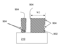
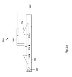
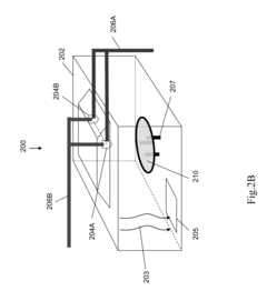
- A vaporizing polymer spray deposition system that atomizes a polymer/solvent solution and deposits a uniform, thin polymer film on semiconductor wafers, filling sharp internal corners and providing a smooth coating using a vaporizing/atomizing spray deposition system.
Methods of fabricating semiconductor structures using thermal spray processes, and semiconductor structures fabricated using such methods
PatentActiveUS9082948B2
Innovation
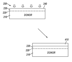
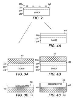
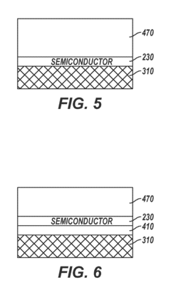
- The method involves forming a weakened zone in a donor structure to create a transfer layer with a substrate layer that closely matches the CTE of the epitaxial layer, providing structural support and enabling the separation of the transfer layer from the donor structure to form a composite substrate with a base substrate layer that matches the CTE of the epitaxial layer, thereby reducing strain and facilitating efficient device formation.
Environmental Impact and Sustainability Considerations
Spray drying processes in semiconductor fabrication present significant environmental challenges that require careful consideration. The high energy consumption associated with these processes contributes substantially to carbon emissions, particularly when powered by non-renewable energy sources. A typical spray drying operation in semiconductor manufacturing consumes between 3-7 kWh per kilogram of processed material, representing a considerable carbon footprint in large-scale production environments.
Water usage presents another critical environmental concern. Conventional spray drying methods require substantial quantities of water for both the slurry preparation and cleaning processes. In water-stressed regions, this consumption pattern raises sustainability questions, especially as semiconductor manufacturing clusters often develop in areas already experiencing water scarcity issues.
Chemical waste management remains a persistent challenge in spray drying applications for semiconductor fabrication. The process generates particulate matter and volatile organic compounds (VOCs) that require sophisticated abatement systems. Recent industry data indicates that approximately 30-40% of chemicals used in these processes become waste streams requiring specialized treatment and disposal.
Regulatory frameworks worldwide are increasingly targeting these environmental impacts. The European Union's Restriction of Hazardous Substances (RoHS) directive and similar regulations in Asia and North America have established stringent requirements for waste management and emissions control in semiconductor manufacturing, directly affecting spray drying operations.
Industry leaders have begun implementing more sustainable approaches to spray drying. Closed-loop water recycling systems have demonstrated potential to reduce freshwater consumption by up to 60% in optimized facilities. Energy recovery systems that capture and reuse thermal energy from exhaust gases can improve energy efficiency by 25-35%, significantly reducing the carbon footprint of these operations.
Alternative, environmentally friendly formulations for semiconductor materials are emerging as promising solutions. Bio-based binders and water-soluble additives that reduce the need for harsh solvents have shown promising results in laboratory settings, though scaling these solutions to production environments remains challenging.
Life cycle assessment (LCA) studies of spray drying in semiconductor applications reveal that the environmental impact extends beyond the manufacturing process itself. The extraction and processing of raw materials used in semiconductor slurries contribute significantly to the overall environmental footprint, highlighting the importance of considering sustainability across the entire supply chain.
Quality Control and Precision Requirements
In semiconductor fabrication, quality control and precision requirements for spray drying methods are exceptionally stringent due to the critical nature of the materials produced. The semiconductor industry demands particle size distributions with extremely narrow tolerances, typically in the submicron range with variations less than ±5%. This level of precision necessitates sophisticated monitoring systems that can provide real-time feedback on critical process parameters.
Temperature and humidity control within spray drying chambers must be maintained within ±1°C and ±2% relative humidity respectively to ensure consistent product quality. Even minor deviations can significantly impact the morphology and electrical properties of the semiconductor materials. Advanced sensor networks employing IoT technology have become standard in modern spray drying facilities, allowing for continuous monitoring of over 20 different process parameters simultaneously.
Contamination control represents another critical aspect of quality management in semiconductor spray drying. Particle contamination levels must typically be maintained below 0.1 particles per cubic foot for particles larger than 0.5 μm. This requires ISO Class 5 (Class 100) or cleaner environments for processing, with regular validation through particle counting and surface analysis techniques. Material purity specifications often exceed 99.9999% (6N purity), necessitating rigorous upstream supplier qualification and incoming material inspection protocols.
Statistical process control (SPC) methodologies have been widely implemented in semiconductor spray drying operations, with control charts monitoring key quality attributes. Process capability indices (Cpk) of 1.33 or higher are typically required for critical parameters, ensuring that processes operate well within specification limits. Advanced analytical techniques including laser diffraction, scanning electron microscopy, and X-ray diffraction are routinely employed for characterization of dried powders.
Automation has become increasingly important in meeting precision requirements, with computer-controlled systems managing process parameters according to predefined recipes. These systems can make micro-adjustments to atomization pressure, feed rates, and drying temperatures in response to real-time measurements, maintaining process stability. Machine learning algorithms are now being deployed to predict quality deviations before they occur, enabling proactive intervention.
Documentation and traceability requirements are particularly stringent, with complete batch records maintained for each production run. These records must include all process parameters, in-process testing results, and final quality certifications. Many semiconductor manufacturers require retention of these records for 5-10 years, allowing for retrospective analysis in case of field failures or performance issues in downstream applications.
Unlock deeper insights with Patsnap Eureka Quick Research — get a full tech report to explore trends and direct your research. Try now!
Generate Your Research Report Instantly with AI Agent
Supercharge your innovation with Patsnap Eureka AI Agent Platform!