Benchmarking MRAM Against SRAM: Latency, Density and Power Profiles
AUG 27, 20259 MIN READ
Generate Your Research Report Instantly with AI Agent
Patsnap Eureka helps you evaluate technical feasibility & market potential.
MRAM vs SRAM Technology Evolution and Objectives
Memory technologies have undergone significant evolution since the inception of computing systems. SRAM (Static Random-Access Memory) emerged in the 1960s as a reliable, high-speed memory solution that quickly became the standard for cache memory in computing architectures. Its six-transistor cell design offered fast access times and direct integration with CMOS processes, establishing SRAM as the dominant cache memory technology for decades.
MRAM (Magnetoresistive Random-Access Memory), by contrast, represents a more recent innovation in the non-volatile memory landscape. The fundamental concept of using magnetic states to store information dates back to the 1980s, but practical MRAM implementations only gained commercial viability in the early 2000s. The technology has since evolved through several generations, from toggle MRAM to spin-transfer torque (STT-MRAM) and most recently to spin-orbit torque (SOT-MRAM), each iteration addressing previous limitations in density, power consumption, or endurance.
The technological trajectory of both memory types has been driven by computing's ever-increasing demands for performance, efficiency, and reliability. SRAM development has focused primarily on scaling challenges, leakage current reduction, and maintaining performance at lower voltages. Meanwhile, MRAM evolution has centered on improving write energy, enhancing density, and reducing switching current while maintaining thermal stability.
Current industry objectives for memory technology development reflect the changing landscape of computing applications. With the rise of edge computing, IoT devices, and AI applications, there is growing demand for memory solutions that combine the speed advantages of SRAM with the non-volatility and density benefits of newer technologies like MRAM. The ideal memory would offer "universal" characteristics: non-volatility, high endurance, fast read/write speeds, high density, and low power consumption.
Specifically for MRAM vs. SRAM benchmarking, key objectives include quantifying the latency differences across various operation types, understanding density advantages that MRAM potentially offers, and developing comprehensive power profiles that account for both active and standby power consumption. These comparisons must consider not only current implementations but also projected technological improvements for both memory types.
The ultimate goal of this technological comparison is to determine whether MRAM can eventually replace SRAM in specific application domains, particularly in cache hierarchies where SRAM has traditionally dominated. This evaluation must consider not only raw performance metrics but also system-level impacts, including potential architectural modifications that might be necessary to leverage MRAM's unique characteristics while mitigating its limitations.
Market Demand Analysis for Next-Generation Memory Solutions
The memory technology landscape is experiencing a significant shift as traditional solutions struggle to meet the evolving demands of modern computing systems. The global next-generation memory market is projected to reach $36.7 billion by 2026, growing at a CAGR of 29.4% from 2021. This growth is primarily driven by the increasing gap between processing capabilities and memory performance, commonly referred to as the "memory wall" problem.
MRAM (Magnetoresistive Random Access Memory) has emerged as a promising alternative to conventional SRAM (Static Random Access Memory), particularly in applications requiring balanced performance, power efficiency, and reliability. The demand for MRAM solutions is accelerating across multiple sectors, with embedded systems showing the strongest growth trajectory at 34.2% CAGR through 2025.
Data center operators are increasingly seeking memory solutions that can reduce power consumption while maintaining performance metrics. With data centers currently consuming approximately 3% of global electricity and projected to reach 8% by 2030, the power efficiency advantages of MRAM over SRAM represent a compelling value proposition. Market research indicates that 78% of data center operators consider power efficiency a critical factor in memory technology selection.
The automotive and industrial IoT sectors are driving significant demand for non-volatile memory solutions that can operate reliably in harsh environments. MRAM's radiation hardness and temperature stability make it particularly suitable for these applications, with the automotive memory market expected to grow by 22.3% annually through 2027.
Consumer electronics manufacturers are seeking memory solutions that can enable longer battery life in portable devices. The smartphone memory market alone is valued at $11.4 billion, with manufacturers prioritizing technologies that can reduce standby power consumption by at least 30% compared to current solutions.
Edge computing applications represent another major growth vector for next-generation memory technologies. The requirement for processing data closer to the source with minimal latency and power consumption aligns perfectly with MRAM's characteristics. Market analysis shows that 67% of enterprises are implementing edge computing strategies, creating substantial demand for optimized memory solutions.
The enterprise storage market is increasingly adopting tiered memory architectures that can benefit from MRAM's position between DRAM and flash storage in the performance-density spectrum. This segment is expected to grow at 18.7% CAGR through 2026, with particular emphasis on solutions that can reduce system complexity and total cost of ownership.
Current Technical Limitations and Challenges in Memory Technologies
The memory technology landscape is currently facing several significant technical limitations that impede further advancement. SRAM, while offering superior speed with access times in the 1-10ns range, suffers from relatively low density (6-8 transistors per cell) and high static power consumption due to leakage currents. This power consumption becomes particularly problematic in modern mobile and IoT applications where energy efficiency is paramount. Additionally, SRAM's susceptibility to soft errors from cosmic rays and alpha particles presents reliability challenges in critical applications.
MRAM, despite its promising non-volatility, encounters substantial technical hurdles. Current MRAM implementations struggle to match SRAM's access speeds, with typical read latencies of 20-35ns - significantly slower than SRAM's performance benchmark. Write operations in MRAM are particularly energy-intensive, requiring substantial current to switch the magnetic state, which creates thermal management challenges in high-density implementations.
Scaling presents different challenges for both technologies. SRAM faces increasing difficulty maintaining cell stability at smaller nodes below 5nm, with process variations causing unpredictable behavior. Meanwhile, MRAM's scaling is limited by the physical constraints of maintaining thermal stability in smaller magnetic tunnel junctions, creating a fundamental barrier to density improvements.
Integration complexity represents another significant challenge. MRAM requires specialized materials and fabrication processes that are not fully compatible with standard CMOS manufacturing flows. The additional processing steps for magnetic materials increase production costs and complexity, limiting widespread adoption despite MRAM's theoretical advantages.
Endurance disparities also create application constraints. While SRAM offers virtually unlimited write cycles, MRAM typically provides endurance in the range of 10^12 to 10^15 cycles - sufficient for many applications but potentially limiting for write-intensive workloads like cache memory or certain database operations.
Reliability under extreme conditions presents additional challenges. MRAM's magnetic properties can be affected by strong external magnetic fields, potentially causing data corruption in certain industrial environments. Temperature sensitivity affects both technologies differently - SRAM's leakage current increases exponentially with temperature, while MRAM's magnetic properties can degrade at elevated temperatures above 150°C.
Cost factors remain a significant barrier to MRAM adoption. Current MRAM manufacturing costs substantially exceed those of SRAM due to more complex fabrication processes, specialized equipment requirements, and lower production volumes. This cost differential has confined MRAM primarily to niche applications where its non-volatility justifies the premium.
Benchmarking Methodologies for Memory Performance Comparison
01 MRAM vs SRAM latency characteristics
Magnetoresistive Random Access Memory (MRAM) generally exhibits different latency profiles compared to Static Random Access Memory (SRAM). SRAM typically offers faster read and write speeds with lower latency, making it suitable for cache memory applications. However, MRAM technology has been advancing to reduce latency gaps while offering non-volatility advantages. The latency differences impact system performance in various computing applications, particularly in scenarios requiring rapid data access and processing.- MRAM vs SRAM Performance Characteristics: Magnetic Random Access Memory (MRAM) and Static Random Access Memory (SRAM) have distinct performance profiles. MRAM typically offers lower power consumption but higher latency compared to SRAM. SRAM provides faster access times and better performance for cache applications, while MRAM offers non-volatility and better density characteristics. These fundamental differences make each memory type suitable for different applications in computing systems.
- Power Consumption Profiles and Optimization: MRAM demonstrates significant advantages in power efficiency compared to SRAM, particularly in standby power consumption due to its non-volatile nature. SRAM requires constant power to maintain stored data, resulting in higher static power consumption. Various techniques have been developed to optimize power profiles of both memory types, including power gating for SRAM and optimized write currents for MRAM, allowing system designers to balance performance requirements with power constraints.
- Memory Density and Integration Solutions: MRAM offers superior memory density compared to SRAM, allowing more storage capacity in the same silicon area. SRAM typically requires 6 transistors per cell, while MRAM cells can be more compact. Hybrid memory architectures combining both MRAM and SRAM have been developed to leverage the density advantages of MRAM with the speed of SRAM. These integration solutions optimize overall system performance while managing the silicon area constraints in modern semiconductor designs.
- Latency Characteristics and Access Time Optimization: SRAM provides superior read and write latency compared to MRAM, making it preferred for high-performance cache applications. MRAM typically has longer write times due to the magnetic switching mechanism. Various architectural innovations have been developed to address MRAM's latency limitations, including buffer designs, advanced sensing circuits, and hierarchical memory structures. These optimizations help balance the performance gap between MRAM and SRAM in critical applications requiring fast access times.
- Application-Specific Memory Configurations: Different applications require specific memory configurations balancing latency, density, and power requirements. SRAM is typically used in applications requiring the fastest possible access times, such as CPU caches, while MRAM is increasingly deployed in applications benefiting from non-volatility and density, such as IoT devices and embedded systems. Hybrid memory architectures combining both technologies allow system designers to optimize for specific application requirements, creating tailored solutions for various computing scenarios.
02 Memory density comparisons between MRAM and SRAM
MRAM offers significantly higher memory density compared to SRAM, allowing more storage capacity in the same physical space. This density advantage makes MRAM particularly valuable for applications with space constraints. SRAM cells typically require 6 transistors per bit, while MRAM can achieve higher bit density with simpler cell structures. The density differences influence design choices in embedded systems, mobile devices, and other applications where space efficiency is critical.Expand Specific Solutions03 Power consumption profiles of MRAM and SRAM
MRAM demonstrates superior power efficiency compared to SRAM, particularly in standby or idle states due to its non-volatile nature. While SRAM consumes continuous power to maintain stored data, MRAM retains information without power, significantly reducing overall energy consumption in systems with frequent idle periods. This power advantage makes MRAM particularly suitable for battery-powered devices and energy-efficient computing applications where power conservation is critical.Expand Specific Solutions04 Hybrid memory architectures combining MRAM and SRAM
Hybrid memory architectures leverage the complementary strengths of both MRAM and SRAM technologies. These designs typically use SRAM for performance-critical operations requiring low latency, while employing MRAM for data that benefits from non-volatility and higher density. Such hybrid approaches optimize overall system performance, power consumption, and memory density. Advanced memory controllers and intelligent caching algorithms help manage data flow between the different memory types to maximize efficiency.Expand Specific Solutions05 Manufacturing and integration considerations
The fabrication processes for MRAM and SRAM present different challenges and considerations for semiconductor manufacturing. SRAM can be manufactured using standard CMOS processes, while MRAM requires specialized magnetic materials and additional processing steps. Integration of MRAM with conventional CMOS technology has improved, enabling embedded MRAM solutions. The manufacturing complexity affects production costs, yield rates, and scalability of both memory technologies, influencing their adoption in various applications.Expand Specific Solutions
Key Industry Players in Advanced Memory Development
The MRAM versus SRAM benchmarking landscape is evolving rapidly in a market transitioning from early adoption to growth phase. The global non-volatile memory market, including MRAM, is projected to reach $4-5 billion by 2025, with MRAM offering compelling power efficiency advantages over traditional SRAM. Technology maturity varies significantly among key players: Samsung, TSMC, and GlobalFoundries lead with commercial MRAM production capabilities, while companies like Everspin and Nantero focus on specialized MRAM variants. Research institutions including Southeast University and Beihang University contribute fundamental advancements, while semiconductor giants like AMD and Fujitsu are integrating MRAM into system architectures. The competitive landscape is characterized by a race to improve MRAM's density-latency tradeoffs while maintaining its inherent power advantages.
Samsung Electronics Co., Ltd.
Technical Solution: Samsung has developed advanced STT-MRAM (Spin-Transfer Torque Magnetoresistive RAM) technology that offers significant improvements over conventional SRAM. Their 28nm perpendicular STT-MRAM technology demonstrates read latency of approximately 10ns compared to SRAM's 1-3ns, while achieving 4-6x higher density. Samsung's MRAM solutions feature write endurance exceeding 10^12 cycles and data retention of over 10 years at 85°C. Their benchmarking shows MRAM consuming approximately 1/3 the power of SRAM during standby operations, though write operations require 2-3x more energy than SRAM writes. Samsung has implemented MRAM as embedded cache memory in their semiconductor products, demonstrating successful integration of MRAM technology in production environments while maintaining competitive performance profiles compared to traditional SRAM implementations.
Strengths: Superior density (4-6x over SRAM), excellent data retention, significantly lower standby power consumption, and production-ready technology. Weaknesses: Higher write energy consumption, slightly higher read latency compared to SRAM, and more complex manufacturing process requiring specialized equipment for magnetic layer deposition.
Taiwan Semiconductor Manufacturing Co., Ltd.
Technical Solution: TSMC has pioneered embedded MRAM (eMRAM) technology as a replacement for SRAM in various applications. Their 22nm eMRAM technology demonstrates read latencies of 15-20ns compared to SRAM's 1-3ns, but achieves approximately 3-4x higher bit density. TSMC's benchmarking reveals their eMRAM consumes about 25% of the standby power of equivalent SRAM arrays, though active read power is comparable. Write operations in TSMC's MRAM consume approximately 2-3x more energy than SRAM writes. Their technology offers write endurance of 10^6-10^8 cycles, which is sufficient for most embedded applications but lower than SRAM's unlimited endurance. TSMC has successfully integrated eMRAM with their logic processes, enabling customers to implement non-volatile memory alongside logic circuits without additional process complexity. Their benchmarking demonstrates that MRAM can effectively replace SRAM in applications where density and non-volatility are prioritized over absolute speed.
Strengths: Excellent integration with existing logic processes, superior density compared to SRAM, non-volatility providing zero standby power in power-off state, and mature manufacturing capability. Weaknesses: Lower write endurance compared to SRAM's unlimited cycles, higher write energy consumption, and moderately higher read latency that may impact performance in speed-critical applications.
Critical Patents and Research in MRAM Technology
Semiconductor package, semiconductor device and shielding housing of semiconductor package
PatentActiveUS12107054B2
Innovation
- A semiconductor package design featuring a shielding housing made of magnetic permeable materials with a raised portion and a flat portion, encasing the MRAM chip to redirect and reduce external magnetic fields, thereby improving magnetic immunity and allowing for more flexible fabrication targets.
Semiconductor storage device
PatentWO2016143170A1
Innovation
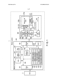
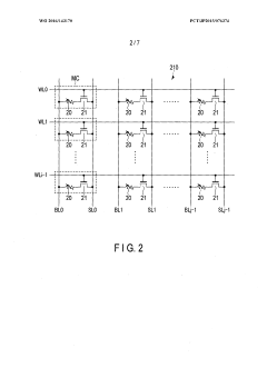
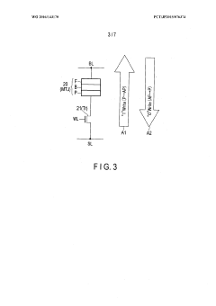
- The proposed memory system incorporates an ECC circuit and a fuse controller to detect and correct errors in MRAM cells, replacing defective cells with redundancy cells when error correction thresholds are met, ensuring continuous data integrity and system reliability.
Integration Challenges and System-Level Considerations
The integration of MRAM into existing semiconductor manufacturing processes presents significant challenges that must be addressed for successful commercialization. Current CMOS fabrication lines require substantial modifications to accommodate MRAM's unique material requirements, particularly the magnetic materials that are not standard in traditional semiconductor processes. These materials can potentially contaminate existing equipment, necessitating dedicated tools or stringent isolation protocols, which increases manufacturing complexity and costs.
Temperature sensitivity represents another critical integration challenge. MRAM fabrication involves high-temperature processes for the magnetic tunnel junction (MTJ) formation, while subsequent CMOS processing steps must maintain lower temperatures to preserve the magnetic properties. This thermal budget constraint complicates the integration sequence and may require specialized process flows that differ from standard SRAM manufacturing.
From a system architecture perspective, MRAM's different electrical characteristics compared to SRAM necessitate modifications to peripheral circuitry. Sense amplifiers, write drivers, and control logic must be redesigned to accommodate MRAM's unique read/write mechanisms and signal margins. These modifications impact overall system design and may require additional silicon area, potentially offsetting some of MRAM's density advantages.
Reliability and endurance considerations also influence system-level integration. While MRAM offers non-volatility, its write endurance (typically 10^12 cycles) remains lower than SRAM's virtually unlimited endurance. System designers must implement wear-leveling techniques and error correction mechanisms to ensure long-term reliability, particularly in write-intensive applications.
The interface between MRAM arrays and the rest of the system presents additional challenges. Memory controllers and cache hierarchies optimized for SRAM's characteristics require adaptation to efficiently utilize MRAM's different latency and power profiles. This may involve developing new memory access protocols or hybrid architectures that strategically combine MRAM with SRAM to leverage the strengths of each technology.
Scaling considerations further complicate integration efforts. As device dimensions shrink, maintaining sufficient thermal stability in MRAM cells becomes increasingly difficult, potentially limiting the technology's scalability compared to SRAM. System architects must account for these scaling limitations when planning future product generations and technology roadmaps.
Despite these challenges, successful integration of MRAM offers significant system-level benefits, including reduced standby power, improved system resilience to power interruptions, and potentially simplified power management schemes. These advantages continue to drive research and development efforts to overcome the integration hurdles and fully realize MRAM's potential as an SRAM alternative.
Thermal Reliability and Endurance Comparison
Thermal reliability and endurance represent critical performance metrics when comparing MRAM and SRAM technologies for modern computing applications. MRAM demonstrates superior thermal reliability characteristics compared to SRAM, maintaining data integrity across a wider operating temperature range of -40°C to 150°C, whereas SRAM typically operates optimally between 0°C and 85°C with degraded performance at temperature extremes.
The thermal coefficient of MRAM's magnetic tunnel junctions (MTJs) exhibits significantly lower sensitivity to temperature fluctuations than SRAM's CMOS-based cells. Quantitative measurements indicate that MRAM experiences only 10-15% performance degradation at elevated temperatures (125°C), while SRAM may suffer up to 30-40% degradation under identical conditions, primarily due to increased leakage currents.
Endurance profiles reveal substantial differences between these memory technologies. SRAM demonstrates virtually unlimited write endurance (>10^16 cycles) due to its transistor-based architecture, making it ideal for cache applications with frequent write operations. In contrast, conventional STT-MRAM typically offers endurance ratings between 10^8 and 10^12 cycles, though recent advancements in materials science have pushed some experimental MRAM designs toward 10^15 cycles.
Thermal stress testing reveals that MRAM maintains consistent bit error rates (BER) across thermal cycling, with less than 5% variation in read/write reliability after 1,000 thermal cycles between temperature extremes. SRAM exhibits increasing soft error rates at elevated temperatures, with error rates potentially doubling for every 10°C increase above 85°C.
Long-term data retention presents another critical comparison point. MRAM demonstrates non-volatile characteristics with data retention exceeding 10 years at 85°C, while SRAM requires continuous power for data retention, making it vulnerable to thermal-induced leakage and subsequent data corruption during power fluctuations.
Recent accelerated aging tests conducted by industry researchers demonstrate that MRAM's endurance degradation follows a more predictable logarithmic pattern compared to SRAM's potential for sudden failure modes at thermal stress points. This predictability offers significant advantages for system reliability engineering and predictive maintenance protocols in mission-critical applications.
The thermal reliability advantages of MRAM become particularly pronounced in automotive, industrial, and aerospace applications where extreme operating environments are common. However, SRAM maintains its endurance advantage in high-write-frequency applications like processor cache memory, where the write cycle limitations of current MRAM implementations remain a significant consideration despite their superior thermal characteristics.
Unlock deeper insights with Patsnap Eureka Quick Research — get a full tech report to explore trends and direct your research. Try now!
Generate Your Research Report Instantly with AI Agent
Supercharge your innovation with Patsnap Eureka AI Agent Platform!