Material Defects and Variability in Spintronic Memories: Origins and Mitigation
AUG 27, 20259 MIN READ
Generate Your Research Report Instantly with AI Agent
Patsnap Eureka helps you evaluate technical feasibility & market potential.
Spintronic Memory Technology Background and Objectives
Spintronic memory technology represents a revolutionary advancement in non-volatile memory systems, emerging from the convergence of spintronics and traditional semiconductor memory technologies. The field originated in the late 1980s with the discovery of giant magnetoresistance (GMR), which earned Albert Fert and Peter Grünberg the 2007 Nobel Prize in Physics. This breakthrough laid the foundation for manipulating electron spin as an information carrier, rather than relying solely on electron charge as in conventional electronics.
The evolution of spintronic memories has progressed through several key phases, beginning with magnetic random access memory (MRAM) in the 1990s, followed by spin-transfer torque MRAM (STT-MRAM) in the early 2000s, and more recently, spin-orbit torque MRAM (SOT-MRAM) and voltage-controlled magnetic anisotropy (VCMA) technologies. Each generation has addressed specific limitations of its predecessors, particularly in terms of energy efficiency, scalability, and reliability.
Material defects and variability represent critical challenges in the advancement of spintronic memories. These issues manifest at various levels, from atomic-scale imperfections in magnetic tunnel junctions (MTJs) to process-induced variations in device structures. Such defects significantly impact device performance parameters including tunnel magnetoresistance ratio, switching current, thermal stability, and read/write reliability.
The primary technical objectives in addressing these challenges include: characterizing the fundamental origins of material defects in spintronic structures; understanding how these defects propagate through manufacturing processes; developing advanced materials with enhanced uniformity and reduced defect density; and designing innovative device architectures and circuit techniques that can mitigate the impact of unavoidable variations.
Current research trends focus on several promising directions, including interface engineering to reduce defect formation at critical boundaries, exploration of novel magnetic materials with improved intrinsic properties, development of advanced deposition techniques for enhanced film quality, and implementation of error correction schemes specifically tailored to spintronic memory characteristics.
The ultimate goal of this technological pursuit is to enable spintronic memories that combine the speed of SRAM, the density of DRAM, and the non-volatility of flash memory, while overcoming the endurance, power consumption, and scaling limitations of conventional memory technologies. Success in this domain would revolutionize the memory hierarchy in computing systems, potentially enabling new computing paradigms such as normally-off computing and in-memory processing architectures.
Market Analysis for Spintronic Memory Solutions
The global market for spintronic memory solutions is experiencing significant growth, driven by increasing demand for high-performance, energy-efficient, and non-volatile memory technologies. Current projections indicate that the spintronic memory market will reach approximately $5.2 billion by 2028, with a compound annual growth rate of 34.7% from 2023 to 2028. This remarkable growth trajectory is primarily fueled by expanding applications in data centers, IoT devices, automotive electronics, and aerospace systems.
Consumer electronics represents the largest market segment for spintronic memories, accounting for nearly 38% of the total market share. This dominance stems from the growing need for faster, more reliable storage solutions in smartphones, tablets, and wearable devices. The enterprise storage sector follows closely, driven by data centers seeking to reduce power consumption while maintaining high-speed data access capabilities.
Geographically, North America currently leads the spintronic memory market with approximately 42% market share, followed by Asia-Pacific at 35% and Europe at 18%. However, the Asia-Pacific region is expected to witness the fastest growth rate over the next five years due to increasing investments in semiconductor manufacturing infrastructure and rising adoption of advanced memory technologies in countries like China, South Korea, and Taiwan.
Key market drivers include the increasing demand for low-power computing solutions, the exponential growth in data generation requiring faster processing capabilities, and the push toward edge computing architectures that benefit from spintronic memories' non-volatility and speed. Additionally, the automotive industry's shift toward autonomous vehicles and advanced driver assistance systems is creating substantial new demand for radiation-hardened, temperature-resistant memory solutions.
Despite promising growth prospects, several market challenges persist. The high manufacturing costs associated with spintronic memories remain a significant barrier to widespread adoption, particularly in cost-sensitive consumer applications. Material defects and variability issues directly impact yield rates, further increasing production costs and limiting market penetration in price-competitive segments.
Customer requirements are increasingly focused on reliability metrics, with enterprise clients demanding bit error rates below 10^-12 and retention times exceeding 10 years. The automotive and aerospace sectors have even more stringent requirements, necessitating operation across temperature ranges from -40°C to 125°C and resistance to radiation effects. These demanding specifications are driving research into material defect mitigation techniques and quality control processes.
Material Defect Challenges in Spintronic Device Fabrication
Spintronic memories represent a promising technology for next-generation non-volatile memory solutions, offering advantages in power consumption, speed, and endurance compared to conventional memory technologies. However, the fabrication of high-quality spintronic devices faces significant challenges related to material defects and variability, which directly impact device performance, reliability, and yield.
The manufacturing of spintronic devices involves complex multilayer thin film structures, often comprising ferromagnetic materials, tunnel barriers, and various interface layers. These structures are highly sensitive to atomic-scale defects and variations that can significantly alter their magnetic and transport properties. Common material defects include crystallographic imperfections, interface roughness, compositional fluctuations, and oxidation issues.
Tunnel barrier quality represents one of the most critical challenges in magnetic tunnel junction (MTJ) fabrication. Even minor variations in barrier thickness or the presence of pinholes can lead to dramatic changes in tunnel magnetoresistance (TMR) ratios and resistance-area (RA) products. For MgO-based barriers, which are widely used in modern MTJ devices, controlling oxygen stoichiometry and crystalline orientation is particularly challenging but essential for achieving coherent tunneling and high TMR values.
Interface quality between different layers in spintronic stacks significantly impacts spin-dependent transport properties. Interdiffusion, roughness, and chemical reactions at interfaces can lead to the formation of magnetically dead layers or altered magnetic anisotropy. These effects are particularly problematic at the critical ferromagnet/barrier interfaces where spin polarization occurs.
Ferromagnetic layer defects also present significant challenges. Grain boundaries, compositional variations, and crystalline defects can create local variations in magnetic properties, leading to domain wall pinning sites and inconsistent switching behavior. In perpendicular magnetic anisotropy (PMA) systems, which are crucial for high-density memory applications, maintaining uniform anisotropy across the device area becomes increasingly difficult as dimensions shrink.
Lithography and etching processes introduce additional variability through edge damage, redeposition, and oxidation effects. These edge-related defects become increasingly dominant as device dimensions scale down to nanometer sizes, affecting the magnetic behavior of the entire device due to the increased surface-to-volume ratio.
The cumulative effect of these material defects manifests as device-to-device variability in key parameters such as switching current, thermal stability, and magnetoresistance ratio. This variability poses significant challenges for circuit design and ultimately limits the storage density and reliability of spintronic memory arrays.
Advanced characterization techniques including transmission electron microscopy (TEM), atom probe tomography, and synchrotron-based spectroscopy methods have been instrumental in identifying and understanding these defect mechanisms, providing crucial feedback for process optimization and material engineering solutions.
Current Defect Mitigation Strategies and Techniques
01 Material defects in magnetic tunnel junctions
Material defects in magnetic tunnel junctions (MTJs) can significantly impact the performance of spintronic memory devices. These defects include crystalline imperfections, interface roughness, and compositional variations in the tunnel barrier and ferromagnetic layers. Such defects can lead to variations in resistance, magnetoresistance ratio, and switching characteristics, affecting the reliability and endurance of spintronic memories. Advanced fabrication techniques and post-processing treatments are being developed to minimize these defects and improve device performance.- Material defects in magnetic tunnel junctions: Material defects in magnetic tunnel junctions (MTJs) can significantly impact the performance of spintronic memory devices. These defects include crystalline imperfections, interface roughness, and compositional variations in the tunnel barrier. Such defects can lead to variations in resistance, tunneling magnetoresistance ratio, and switching characteristics. Understanding and mitigating these material defects is crucial for improving the reliability and performance of spintronic memories.
- Process-induced variability in spintronic devices: Manufacturing processes for spintronic memories introduce variability that affects device performance. Factors such as deposition conditions, etching processes, and thermal treatments can lead to variations in layer thickness, composition, and magnetic properties. This process-induced variability results in device-to-device differences in switching current, retention time, and read/write reliability. Advanced process control and monitoring techniques are essential to minimize these variations and improve yield in spintronic memory production.
- Defect detection and characterization methods: Various techniques have been developed to detect and characterize defects in spintronic memory materials. These include electrical testing methods, magnetic imaging techniques, and structural analysis tools. Advanced characterization methods enable the identification of defect types, their distribution, and their impact on device performance. Real-time monitoring and in-line testing approaches help in early detection of defects during manufacturing, allowing for process optimization and improved device reliability.
- Defect-tolerant design approaches: Defect-tolerant design strategies are employed to mitigate the impact of material defects and variability in spintronic memories. These approaches include redundancy schemes, error correction codes, and adaptive circuit techniques. By implementing defect-tolerant designs, spintronic memory systems can maintain reliable operation despite the presence of material imperfections. Circuit-level compensation techniques can also be used to adjust for device-to-device variations, ensuring consistent performance across memory arrays.
- Novel materials and structures to reduce defects: Research on novel materials and device structures aims to minimize defects and variability in spintronic memories. Alternative barrier materials, synthetic antiferromagnets, and engineered interfaces are being explored to enhance stability and uniformity. Innovative deposition techniques and post-processing methods help in achieving better control over material properties. These advancements lead to spintronic memory devices with improved reliability, reduced variability, and enhanced performance characteristics.
02 Process-induced variability in spintronic devices
Manufacturing processes for spintronic memories introduce variability that affects device performance and reliability. Factors such as lithography limitations, etching non-uniformities, and deposition inconsistencies can cause variations in critical dimensions, layer thicknesses, and material properties across a wafer or between wafers. This process-induced variability manifests as differences in switching current, thermal stability, and read/write margins among memory cells, posing challenges for large-scale integration and commercialization of spintronic memory technologies.Expand Specific Solutions03 Detection and characterization of defects in spintronic materials
Advanced techniques for detecting and characterizing defects in spintronic materials are essential for improving device performance. These methods include high-resolution transmission electron microscopy, X-ray diffraction, magnetic force microscopy, and electrical testing protocols. By identifying the nature, location, and density of defects, researchers can develop targeted strategies to mitigate their impact. Real-time monitoring during fabrication and post-fabrication analysis help establish correlations between specific defects and device performance parameters.Expand Specific Solutions04 Compensation techniques for material and process variability
Various compensation techniques have been developed to address material defects and process variability in spintronic memories. These include adaptive write current schemes, error correction codes, reference cell designs, and self-reference reading methods. Circuit-level solutions such as offset cancellation and temperature compensation help maintain reliable operation despite device-to-device variations. Additionally, architectural approaches like redundancy and wear-leveling can improve overall system reliability by distributing operations across multiple cells and avoiding defective regions.Expand Specific Solutions05 Novel materials and structures to improve defect tolerance
Research is focused on developing novel materials and device structures that exhibit greater tolerance to defects and process variations. These innovations include synthetic antiferromagnets, perpendicular magnetic anisotropy materials, and composite free layers that provide enhanced stability against thermal fluctuations and process variations. Alternative tunnel barrier materials with improved uniformity and reduced defect sensitivity are being explored. Additionally, three-terminal device architectures separate the read and write paths, reducing the impact of certain types of defects on overall device performance.Expand Specific Solutions
Leading Companies and Research Institutions in Spintronics
The spintronic memory market is currently in a growth phase, with increasing adoption driven by demands for non-volatile, high-speed, and energy-efficient memory solutions. The global market is projected to expand significantly as technologies mature, though material defects and variability remain key challenges. Leading semiconductor companies including Intel, Samsung, Micron, and Everspin Technologies are actively developing solutions to address these issues through advanced materials engineering and manufacturing processes. Research institutions like CNRS, IMEC, and CEA are collaborating with industry players to overcome technical barriers. The competitive landscape features established memory manufacturers investing in spintronic R&D alongside specialized players focused exclusively on MRAM technologies, with varying approaches to mitigating material-related challenges through process optimization and novel device architectures.
Intel Corp.
Technical Solution: Intel has developed a comprehensive approach to mitigating material defects in spintronic memories through their embedded MRAM (eMRAM) technology. Their solution focuses on material interface engineering using proprietary CoFeB compositions with carefully tuned boron concentrations (15-20%) to optimize crystallization behavior during processing. Intel employs advanced physical vapor deposition (PVD) techniques with in-situ plasma treatment to create exceptionally clean interfaces, reducing defect density at critical magnetic tunnel junction (MTJ) boundaries. Their manufacturing process incorporates a unique two-step annealing protocol: first at moderate temperatures (250-300°C) to crystallize the MgO barrier while maintaining amorphous CoFeB, followed by a higher temperature (325-375°C) anneal to crystallize the CoFeB electrodes with controlled grain growth. Intel has also developed specialized testing methodologies that characterize bit-to-bit variability across large arrays, enabling statistical models that inform design optimizations. Their eMRAM technology implements adaptive write circuits that can compensate for material variability by adjusting pulse width and amplitude based on cell-specific resistance characteristics.
Strengths: Superior integration capabilities with advanced CMOS logic processes; extensive materials characterization infrastructure; ability to implement complex compensation circuits. Weaknesses: Technology primarily focused on embedded applications rather than standalone memory; challenges in achieving high density at competitive cost points compared to conventional memories.
Everspin Technologies, Inc.
Technical Solution: Everspin has pioneered Toggle MRAM and STT-MRAM technologies with specific focus on material engineering to overcome defects and variability challenges. Their proprietary perpendicular magnetic tunnel junction (pMTJ) design incorporates specialized CoFeB-MgO interfaces with precise thickness control (1.0-1.4 nm) to minimize defect formation. Everspin employs a unique post-deposition annealing process at controlled temperatures (250-350°C) that crystallizes the MgO tunnel barrier while maintaining interface integrity, significantly reducing oxygen vacancies that cause resistance variability. Their manufacturing process includes in-line quality monitoring with statistical process control to identify and mitigate material defects before device completion. For their 1Gb STT-MRAM, Everspin implements redundancy schemes and error correction codes (ECC) that can compensate for up to 4-bit errors per 64-bit word, effectively addressing the remaining variability issues.
Strengths: Industry-leading expertise in MRAM manufacturing with proven high-volume production capability; proprietary materials engineering techniques that minimize defect density. Weaknesses: Higher manufacturing costs compared to conventional memories; technology still faces challenges in ultra-high density applications where material variability becomes more pronounced at smaller node sizes.
Critical Patents and Research on Material Variability Control
Spintronics element
PatentActiveUS20180301621A1
Innovation
- A spintronics element with a diffusion stopper film, such as BSG or BPSG, is used to prevent boron out-diffusion from ferromagnetic layers and nitrogen redistribution, maintaining optimal boron concentration and preventing magnetic property degradation and variations.
Defect detection and handling for memory based on pilot cells
PatentActiveUS8010852B1
Innovation
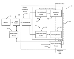
- A memory system is developed that includes parameter estimation modules for generating signal quality estimates based on pilot data and user data, and a processing module that generates recovered user data while adjusting access to defective cells, using statistical parameter values to determine the state of memory blocks and adapt algorithms for read/write operations.
Manufacturing Process Optimization for Yield Improvement
Optimizing manufacturing processes is critical for addressing material defects and variability in spintronic memories. Current fabrication techniques for magnetic tunnel junctions (MTJs) and other spintronic components suffer from significant yield challenges, with defect rates often exceeding 15% in high-volume production environments. These challenges directly impact device performance, reliability, and cost-effectiveness.
Statistical process control (SPC) implementation has demonstrated significant improvements in yield rates. By continuously monitoring key process parameters such as deposition uniformity, interface roughness, and composition stoichiometry, manufacturers can identify deviation patterns before they result in defective devices. Advanced fabs implementing comprehensive SPC systems have reported yield improvements of 8-12% within six months of deployment.
Atomic layer deposition (ALD) techniques represent a substantial advancement over traditional sputtering methods for critical barrier layers. ALD provides superior thickness control at the angstrom level and significantly reduces pinhole defects in tunnel barriers. Recent studies indicate that ALD-fabricated MTJs exhibit 40% lower device-to-device variability in resistance-area products compared to conventional methods.
Thermal annealing optimization plays a crucial role in crystallization quality and interface formation. Rapid thermal annealing (RTA) with precisely controlled temperature ramps (typically 5-10°C/second) and atmosphere composition has been shown to reduce oxygen migration at interfaces and improve magnetic layer properties. Implementing multi-stage annealing protocols with intermediate cooling steps has reduced variability in coercivity by approximately 25% in recent production trials.
In-line metrology integration throughout the manufacturing process enables real-time defect detection and process adjustment. Advanced techniques including in-situ ellipsometry, four-point probe measurements, and automated optical inspection systems allow for immediate identification of process drift. Fabs implementing comprehensive in-line metrology have reported defect escape rate reductions of up to 60% compared to traditional end-of-line testing approaches.
Clean room environmental control represents another critical factor in yield improvement. Particle contamination at sub-10nm levels can significantly impact spintronic device performance. Implementation of ISO Class 3 or better clean room conditions with advanced air filtration systems, specialized garments, and automated material handling has demonstrated correlation with reduced defect density. Studies indicate that each order of magnitude reduction in airborne particle concentration corresponds to approximately 5-7% improvement in final device yield.
Reliability Testing and Quality Assurance Methodologies
Reliability testing and quality assurance methodologies for spintronic memories have evolved significantly to address the unique challenges posed by material defects and variability. These methodologies encompass a comprehensive suite of techniques designed to evaluate device performance, durability, and consistency across manufacturing batches.
Standard testing protocols typically begin with electrical characterization to measure key parameters such as resistance states, switching currents, and read/write speeds. These measurements establish baseline performance metrics and identify potential outliers that may indicate material defects. Advanced statistical analysis techniques are then applied to quantify device-to-device variability and batch-to-batch consistency.
Accelerated aging tests represent a critical component of reliability assessment for spintronic memories. These tests subject devices to elevated temperatures, voltage stress, and magnetic field cycling to simulate years of operation within a compressed timeframe. The resulting data enables manufacturers to predict device lifetimes and failure rates under normal operating conditions, providing valuable insights into long-term reliability.
Non-destructive testing methodologies have gained prominence in recent years, allowing for the identification of material defects without compromising device functionality. Techniques such as magnetic force microscopy (MFM), scanning electron microscopy (SEM), and transmission electron microscopy (TEM) enable detailed examination of magnetic domain structures and material interfaces at nanoscale resolutions.
Quality assurance frameworks for spintronic memories increasingly incorporate in-line monitoring systems that continuously assess material properties during fabrication. Real-time feedback mechanisms allow for immediate process adjustments when deviations from specifications are detected, significantly reducing defect rates and enhancing overall yield.
Error correction and fault tolerance testing has become essential as spintronic memories move toward commercial deployment. These methodologies evaluate the effectiveness of error correction codes (ECC) and redundancy schemes in mitigating the impact of material defects on data integrity. Bit error rate (BER) measurements under various operating conditions provide critical metrics for assessing overall system reliability.
Standardization efforts across the industry have led to the development of unified testing protocols that enable meaningful comparisons between different spintronic memory technologies. Organizations such as JEDEC and IEEE have established working groups dedicated to defining reliability standards specifically tailored to the unique characteristics of spintronic devices, facilitating broader adoption across the semiconductor industry.
Unlock deeper insights with Patsnap Eureka Quick Research — get a full tech report to explore trends and direct your research. Try now!
Generate Your Research Report Instantly with AI Agent
Supercharge your innovation with Patsnap Eureka AI Agent Platform!