How to Engineer Magnetic Tunnel Junctions for Spintronic Storage Applications
AUG 27, 20259 MIN READ
Generate Your Research Report Instantly with AI Agent
Patsnap Eureka helps you evaluate technical feasibility & market potential.
MTJ Technology Background and Objectives
Magnetic Tunnel Junctions (MTJs) have emerged as a pivotal technology in the field of spintronics, representing a significant advancement beyond conventional electronic devices that rely solely on electron charge. The evolution of MTJ technology can be traced back to the discovery of Giant Magnetoresistance (GMR) in the late 1980s, which earned Albert Fert and Peter Grünberg the Nobel Prize in Physics in 2007. This breakthrough laid the foundation for the development of Tunnel Magnetoresistance (TMR) and subsequently MTJs, which have shown remarkable potential for non-volatile memory applications.
The fundamental structure of an MTJ consists of two ferromagnetic layers separated by an ultrathin insulating barrier, typically made of magnesium oxide (MgO). The resistance of this junction varies significantly depending on the relative magnetization directions of the ferromagnetic layers, a phenomenon known as tunnel magnetoresistance. This binary resistance state forms the basis for data storage in spintronic devices, offering advantages such as non-volatility, high speed, and low power consumption.
Over the past decade, MTJ technology has progressed through several generations, each marked by improvements in materials, fabrication techniques, and device architectures. Early MTJs utilized aluminum oxide barriers, which have since been replaced by crystalline MgO barriers, resulting in significantly higher TMR ratios. Recent advancements have focused on perpendicular magnetic anisotropy (PMA) materials, which enable higher storage densities and improved thermal stability.
The primary objective in MTJ engineering for spintronic storage applications is to achieve an optimal balance between several critical parameters: high TMR ratio for clear signal distinction, low switching current for energy efficiency, high thermal stability for data retention, and fast switching speed for competitive performance. Additionally, scalability to dimensions below 20nm is essential for meeting the demands of high-density storage applications.
Current research aims to overcome several technical challenges, including reducing the critical switching current density while maintaining thermal stability, enhancing endurance to withstand numerous write cycles, and developing manufacturing processes compatible with existing semiconductor fabrication techniques. The integration of MTJs with CMOS technology represents another significant goal, as it would enable the creation of hybrid memory-logic devices with unprecedented capabilities.
The long-term vision for MTJ technology extends beyond conventional memory applications to include neuromorphic computing architectures, where MTJs could serve as artificial synapses or neurons. This potential application aligns with the growing interest in brain-inspired computing systems that offer superior energy efficiency for specific tasks such as pattern recognition and data classification.
Spintronic Storage Market Analysis
The global spintronic storage market is experiencing robust growth, driven by increasing demand for high-density data storage solutions with enhanced performance characteristics. Current market valuations place the spintronic storage sector at approximately 1.5 billion USD in 2023, with projections indicating a compound annual growth rate (CAGR) of 34% through 2030, potentially reaching 9.8 billion USD by the end of the decade.
The primary market drivers include the exponential growth in data generation across various sectors, particularly cloud computing, artificial intelligence, and Internet of Things (IoT) applications. These technologies require storage solutions that offer faster access times, lower power consumption, and greater reliability than conventional storage technologies—attributes that spintronic storage devices, particularly those based on Magnetic Tunnel Junctions (MTJs), can deliver.
Enterprise data centers represent the largest market segment, accounting for 42% of current spintronic storage adoption. This is followed by consumer electronics at 28%, automotive applications at 15%, and industrial systems at 10%, with other applications comprising the remaining 5%. Geographically, North America leads with 38% market share, followed by Asia-Pacific at 35%, Europe at 22%, and other regions at 5%.
The competitive landscape features both established semiconductor giants and specialized startups. Major players include Samsung Electronics, Intel, Toshiba, and Western Digital, who are investing heavily in spintronic R&D. Meanwhile, specialized companies like Everspin Technologies and Spin Memory are focusing exclusively on MTJ-based memory solutions, gaining significant traction through technological innovation despite their smaller size.
Market challenges include high manufacturing costs, with current MTJ-based storage solutions commanding a premium of 2.5-3x over conventional NAND flash memory. Technical hurdles in scaling MTJ devices below 10nm while maintaining thermal stability also present commercialization barriers. Additionally, integration challenges with existing CMOS processes increase production complexity and costs.
Customer demand analysis reveals strong interest in spintronic storage's non-volatility and radiation hardness for aerospace and military applications. The automotive sector is increasingly adopting these technologies for advanced driver-assistance systems (ADAS) and autonomous vehicles, where conventional storage solutions struggle with temperature extremes and reliability requirements.
Future market growth will likely be catalyzed by breakthroughs in MTJ engineering that address current scaling and manufacturing challenges, potentially disrupting the 120 billion USD global memory market if cost parity with conventional technologies can be achieved.
Current MTJ Development Status and Challenges
Magnetic Tunnel Junctions (MTJs) have emerged as the cornerstone technology for spintronic storage applications, with significant advancements achieved over the past two decades. Currently, the industry has successfully commercialized MTJ-based Magnetoresistive Random Access Memory (MRAM) products, demonstrating the technology's viability. Leading semiconductor manufacturers including Samsung, TSMC, and Intel have integrated MTJ technology into their production lines, with devices exhibiting tunnel magnetoresistance (TMR) ratios exceeding 200% at room temperature.
Despite these achievements, several critical challenges persist in MTJ engineering. The foremost challenge involves the delicate balance between thermal stability and switching current density. As device dimensions shrink below 20nm to meet high-density storage requirements, maintaining sufficient thermal stability factor (Δ) above 60 becomes increasingly difficult while simultaneously requiring manageable switching currents for energy efficiency.
Material engineering represents another significant hurdle. Current CoFeB/MgO-based MTJs face limitations in achieving TMR ratios beyond 600%, which constrains read margins in high-speed applications. The industry is actively exploring alternative material systems, including Heusler alloys and topological insulators, though these materials present complex fabrication challenges and integration issues with CMOS processes.
Reliability and endurance remain persistent concerns, with current MTJ technologies typically demonstrating endurance of 10^12 cycles, falling short of the 10^16 cycles required to fully compete with conventional memory technologies. Write error rates and read disturbance also increase dramatically at reduced dimensions and faster operating speeds, necessitating sophisticated error correction mechanisms.
Manufacturing scalability presents substantial obstacles, particularly in achieving consistent MTJ performance across wafers. The precise control of layer thicknesses at angstrom scales and maintaining interface quality during high-temperature CMOS back-end processing (typically exceeding 400°C) remain significant challenges. Current yields for advanced MTJ processes typically range from 85-92%, below the 99%+ standards of mature memory technologies.
From a geographical perspective, MTJ technology development shows distinct regional characteristics. Japan and South Korea lead in fundamental materials research and patent filings, while the United States dominates in design architecture and integration techniques. China has recently accelerated investments in this field, particularly focusing on novel materials and alternative switching mechanisms.
The academic-industrial collaboration landscape has intensified, with research consortia forming around key technical challenges. Notable initiatives include the IMEC spintronics program in Europe and the JUMP 2.0 program in the United States, both targeting next-generation MTJ solutions for beyond-CMOS computing paradigms.
Current MTJ Engineering Solutions
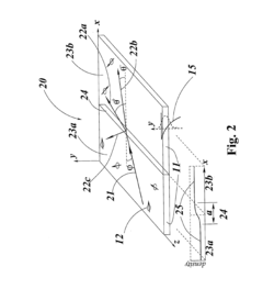
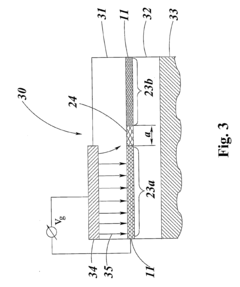
01 Structure and fabrication of magnetic tunnel junctions
Magnetic tunnel junctions (MTJs) consist of two ferromagnetic layers separated by a thin insulating barrier. The fabrication process involves depositing multiple layers of materials, including magnetic materials and tunnel barriers, using techniques such as sputtering or molecular beam epitaxy. The structure can be optimized by controlling the thickness and composition of each layer to enhance performance characteristics such as tunnel magnetoresistance ratio and thermal stability.- Structure and fabrication of magnetic tunnel junctions: Magnetic tunnel junctions (MTJs) consist of two ferromagnetic layers separated by a thin insulating barrier. The fabrication process involves depositing multiple layers of materials, including magnetic materials and tunnel barriers, using techniques such as sputtering or molecular beam epitaxy. The structure can be optimized by controlling the thickness and composition of each layer to enhance performance characteristics such as tunnel magnetoresistance ratio and thermal stability.
- Materials for enhancing MTJ performance: Various materials are used in magnetic tunnel junctions to improve performance metrics. These include MgO barriers for high tunnel magnetoresistance, CoFeB electrodes for enhanced spin polarization, and synthetic antiferromagnetic structures for improved stability. Material engineering focuses on optimizing interfaces between layers and developing novel material combinations to achieve higher magnetoresistance ratios, lower switching currents, and better thermal stability.
- Applications in memory and computing devices: Magnetic tunnel junctions serve as the fundamental building blocks for various spintronic devices, particularly in non-volatile memory applications such as Magnetoresistive Random Access Memory (MRAM) and Spin-Transfer Torque MRAM (STT-MRAM). They are also being developed for neuromorphic computing systems, magnetic sensors, and logic devices. These applications leverage the non-volatility, high speed, and low power consumption characteristics of MTJs to create more efficient computing architectures.
- Switching mechanisms in MTJs: Various mechanisms are employed to switch the magnetization state in magnetic tunnel junctions. These include field-induced switching, spin-transfer torque (STT), spin-orbit torque (SOT), and voltage-controlled magnetic anisotropy (VCMA). Each mechanism offers different advantages in terms of energy efficiency, switching speed, and scalability. Recent developments focus on reducing the critical current needed for switching while maintaining thermal stability and reliability.
- Integration and scaling of MTJ technology: Integration of magnetic tunnel junctions with CMOS technology presents challenges in terms of process compatibility, thermal budgets, and scaling. Solutions include developing back-end-of-line compatible processes, creating novel cell architectures for higher density, and implementing advanced patterning techniques to achieve smaller feature sizes. Scaling efforts focus on maintaining performance while reducing device dimensions to compete with conventional memory technologies.
02 MTJ applications in memory devices
Magnetic tunnel junctions serve as the fundamental building blocks for various memory technologies, particularly Magnetoresistive Random Access Memory (MRAM) and Spin-Transfer Torque MRAM (STT-MRAM). These memory devices offer advantages such as non-volatility, high endurance, fast read/write speeds, and low power consumption. MTJs in memory applications can be integrated with CMOS technology to create high-density storage solutions for various computing applications.Expand Specific Solutions03 Enhancement of MTJ performance characteristics
Various techniques can be employed to enhance the performance of magnetic tunnel junctions, including the use of perpendicular magnetic anisotropy materials, synthetic antiferromagnetic structures, and novel barrier materials. These enhancements aim to improve key parameters such as the tunnel magnetoresistance ratio, switching current density, thermal stability, and read/write reliability. Advanced material engineering and interface control are critical for optimizing these performance characteristics.Expand Specific Solutions04 MTJ integration with semiconductor devices
Integration of magnetic tunnel junctions with semiconductor devices involves addressing challenges related to process compatibility, thermal budgets, and electrical interconnections. Various approaches include back-end-of-line integration, 3D stacking, and monolithic integration. These integration strategies enable the development of hybrid memory-logic circuits, neuromorphic computing elements, and other advanced electronic systems that leverage both magnetic and semiconductor properties.Expand Specific Solutions05 Sensing and detection applications of MTJs
Magnetic tunnel junctions can be utilized in various sensing applications, including magnetic field sensors, current sensors, and position detectors. The high sensitivity of MTJs to magnetic fields makes them suitable for applications requiring precise detection of magnetic signals. These sensing capabilities can be leveraged in automotive systems, industrial equipment, biomedical devices, and other fields where accurate magnetic field detection is required.Expand Specific Solutions
Leading Companies in Spintronics Industry
The magnetic tunnel junction (MTJ) technology for spintronic storage applications is currently in a transitional phase from research to commercialization, with an estimated market size of $1.5-2 billion and projected annual growth of 35%. The competitive landscape features established semiconductor giants like Samsung, Micron, and TSMC focusing on integration with existing memory technologies, while research institutions such as CEA, CNRS, and Beihang University drive fundamental innovation. IBM and Qualcomm lead in patenting activity, with IBM demonstrating significant advancements in MTJ reliability and performance. Asian manufacturers, particularly SK Hynix and SMIC, are rapidly scaling production capabilities, while specialized players like Headway Technologies focus on niche applications requiring high-performance spintronic solutions.
Commissariat à l´énergie atomique et aux énergies Alternatives
Technical Solution: CEA has developed advanced perpendicular magnetic tunnel junctions (p-MTJs) utilizing CoFeB/MgO interfaces with enhanced tunnel magnetoresistance (TMR) ratios exceeding 200% at room temperature. Their approach focuses on optimizing the crystalline structure of the MgO barrier through precise deposition techniques and post-annealing processes to achieve coherent tunneling. CEA's technology incorporates synthetic antiferromagnetic (SAF) reference layers to enhance thermal stability and reduce stray fields. They've pioneered the integration of voltage-controlled magnetic anisotropy (VCMA) effects to reduce switching current densities by up to 50%, significantly improving energy efficiency. Their MTJ stacks feature perpendicular magnetic anisotropy (PMA) that enables scaling below 20nm diameter while maintaining thermal stability factors above 60, essential for 10-year data retention in MRAM applications.
Strengths: Superior TMR ratios enabling clear read signals; excellent scalability to sub-20nm nodes; reduced power consumption through VCMA implementation. Weaknesses: Complex multi-layer deposition process requiring precise control; potential reliability challenges at elevated temperatures; higher manufacturing costs compared to conventional memory technologies.
Samsung Electronics Co., Ltd.
Technical Solution: Samsung has engineered high-performance magnetic tunnel junctions using a sophisticated CoFeB/MgO/CoFeB structure with perpendicular magnetic anisotropy (PMA). Their proprietary stack design incorporates ultra-thin CoFeB layers (1.0-1.4nm) with optimized Fe:Co ratios to maximize interfacial anisotropy at the CoFeB/MgO interface. Samsung's MTJs achieve tunnel magnetoresistance ratios exceeding 250% through careful control of MgO crystallization and interface quality. They've developed a unique two-step annealing process: first at moderate temperature (300°C) to initiate crystallization, followed by a higher temperature anneal (400°C) with applied magnetic field to optimize the reference layer. Their technology employs synthetic antiferromagnetic (SAF) structures with Ru spacers precisely tuned to 0.85nm to ensure strong antiferromagnetic coupling. Samsung has also pioneered the integration of strain-engineering techniques, introducing slight lattice distortions to enhance PMA and reduce switching current by approximately 30%.
Strengths: Industry-leading TMR ratios; excellent thermal stability (Δ>70) enabling 10+ year data retention; proven manufacturing scalability to 28nm node with roadmap to 15nm. Weaknesses: Relatively high process complexity requiring specialized deposition equipment; sensitivity to process variations affecting yield; higher switching currents compared to emerging SOT-MRAM approaches.
Key MTJ Materials and Interface Physics
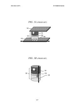
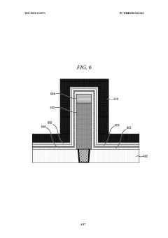
Magnetic tunnel junction having all-around structure
PatentWO2021123971A1
Innovation
- The MTJ structure is redesigned with an all-around configuration where ferromagnetic layers and the barrier layer concentrically surround a central conductor, increasing the interface area between the free layer and spin orbit torque (SOT) metal, thereby enhancing switching efficiency.


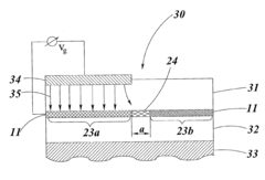
Device and method for manipulating direction of motion of current carriers
PatentInactiveUS20110037512A1
Innovation
- A device and method utilizing a two-dimensional gas of current carriers with regions of inhomogeneity in spin-orbit coupling constant and density, allowing for spin-dependent refraction, reflection, and diffraction, and enabling the manipulation of current carriers through lateral interfaces and diffusive-ballistic transitions to achieve desired direction changes and polarization.
Manufacturing Scalability Considerations
The scalability of manufacturing processes for Magnetic Tunnel Junctions (MTJs) represents a critical factor in their commercial viability for spintronic storage applications. Current fabrication techniques face significant challenges when transitioning from laboratory-scale production to high-volume manufacturing environments. The primary obstacle lies in maintaining precise control over nanometer-scale features while achieving consistent performance across millions of devices on a single wafer.
Deposition uniformity emerges as a fundamental concern, particularly for the ultra-thin tunnel barrier layer, typically composed of MgO with a thickness of 1-2 nm. Even minor variations in this layer can dramatically alter the tunnel magnetoresistance (TMR) ratio and device reliability. Advanced physical vapor deposition (PVD) systems with improved target utilization and enhanced plasma control have demonstrated promising results in addressing this challenge, achieving thickness variations below 2% across 300mm wafers.
Lithography resolution presents another significant manufacturing hurdle. As MTJ dimensions continue to shrink below 30nm to increase storage density, conventional optical lithography approaches their physical limits. Extreme ultraviolet (EUV) lithography offers a potential solution, though its implementation introduces additional cost considerations. Alternatively, directed self-assembly (DSA) techniques combined with conventional lithography show promise for cost-effective patterning of high-density MTJ arrays.
Etching processes for MTJ stacks require exceptional precision due to the complex multilayer structure containing diverse materials. Ion beam etching (IBE) remains the predominant approach, though issues with redeposition and sidewall damage persist. Recent developments in reactive ion etching (RIE) with carefully tailored chemistry show improved profile control and reduced damage to the magnetic properties of the stack.
Post-fabrication annealing represents a critical step for crystallizing the MgO barrier and establishing proper magnetic ordering. However, scaling this process introduces thermal budget challenges and potential for interlayer diffusion. Rapid thermal annealing (RTA) systems with enhanced temperature uniformity and precise atmosphere control have demonstrated improvements in device-to-device consistency across large wafers.
Integration with CMOS backend processes introduces additional complexity, particularly regarding thermal budget constraints and contamination control. The development of low-temperature deposition techniques and effective diffusion barriers has proven essential for maintaining CMOS compatibility while preserving MTJ performance characteristics. Recent advances in equipment design have enabled better isolation of magnetic materials processing from standard CMOS fabrication lines.
Energy Efficiency and Thermal Stability Analysis
Energy efficiency and thermal stability represent two critical parameters in the engineering of Magnetic Tunnel Junctions (MTJs) for spintronic storage applications. The power consumption of MTJ-based devices directly impacts their viability in modern computing systems, particularly in mobile and IoT applications where energy constraints are significant. Current MTJ designs typically require 10-100 μA of switching current, which, while lower than conventional memory technologies, still presents opportunities for optimization.
The fundamental energy efficiency challenge in MTJs stems from the trade-off between thermal stability and switching energy. Higher thermal stability factors (Δ) necessitate larger switching currents, creating an inherent conflict in design objectives. Recent advancements in perpendicular magnetic anisotropy (PMA) materials have demonstrated promising results, reducing switching energies to sub-fJ levels while maintaining acceptable stability parameters.
Thermal stability, quantified by the factor Δ = KuV/kBT (where Ku is the anisotropy constant, V is the volume, kB is the Boltzmann constant, and T is temperature), must typically exceed 40-60 for reliable data retention in commercial applications. This requirement becomes increasingly challenging as device dimensions shrink below 20nm, where thermal fluctuations can more easily overcome the energy barrier between magnetization states.
Several innovative approaches are being explored to address these challenges. Interface engineering techniques, such as inserting ultrathin layers of heavy metals or oxides at the CoFeB/MgO interface, have shown potential to enhance PMA without compromising tunneling magnetoresistance (TMR). These modifications can increase thermal stability while maintaining reasonable switching currents.
Shape engineering represents another promising direction, with elliptical or synthetic antiferromagnetic (SAF) free layer structures demonstrating improved stability-to-switching energy ratios compared to conventional circular designs. The incorporation of voltage-controlled magnetic anisotropy (VCMA) effects has also emerged as a potential pathway to reduce switching energy by temporarily modifying the energy barrier during write operations.
Thermal management strategies are increasingly important as device densities increase. Heat dissipation through optimized electrode materials and integration schemes can prevent performance degradation and extend device lifetimes. Recent studies indicate that thermal conductivity of the surrounding materials can significantly impact MTJ performance, with up to 30% variation in switching characteristics observed under different thermal conditions.
The development of advanced characterization techniques, including time-resolved measurements and in-situ thermal imaging, has been crucial in understanding the complex interplay between energy efficiency and thermal stability in practical device implementations. These insights are driving the next generation of MTJ designs toward the theoretical limits of energy efficiency while maintaining the reliability required for commercial storage applications.
Unlock deeper insights with Patsnap Eureka Quick Research — get a full tech report to explore trends and direct your research. Try now!
Generate Your Research Report Instantly with AI Agent
Supercharge your innovation with Patsnap Eureka AI Agent Platform!